- Products
- Products
- Companies
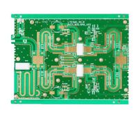
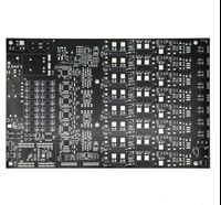
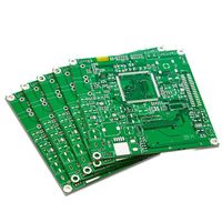
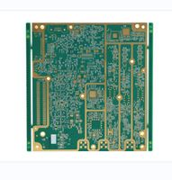
Difficult immersion gold double-sided electronic OEM customized product 4G 5G smart phone blind hole HDI board

-
Supplier: Jinhua Technology (Shenzhen) Co., Ltd. -
Region: Guangdong, China -
Contact: Ms Rosia Cao -
Price: $3.50 / 1 - 999 pieces
$1.50 / 1000 - 4999 pieces
$0.50 / 5000 - 9999 pieces
$0.10 / >=10000 pieces -
Min. Order: 1 piece
| Key words: | Immersion Gold High Density PCB | product name: | High Density PCB |
| application: | electronic product | payment terms: | L/C, Western Union, D/P, D/A, T/T, MoneyGram |
| Surface treatment: | Electroless Nickel Gold | Certificate: | ISO9001/ISO14001/CE/ROHS |
| Packaging Details: | Bubble packaging, pearl cotton packaging, anti-static bags, vacuum bags | Substrate: | FR4,FR4 |
| minute. Line spacing: | 3 million | minute. line width: | 3 million |
| minute. Hole size: | 0.15 mm | brand: | Jinhua |
| Copper thickness: | 1 oz | model: | JH-HDI-033 |
| Package preview: | Supply capacity: | 60000 pieces per month | |
| port: | Shenzhen | type: | HD PCB |
| Origin: | Guangdong, China | Plate thickness: | Can be customized, 1.6mm |
| MOQ: | 1 | Serve: | Multi-layer immersion gold high-density PCB service |
| Test service: | 100% AOI testing | layer: | 1~20 floors |
| Board size: | 300*600mm, or can be customized |
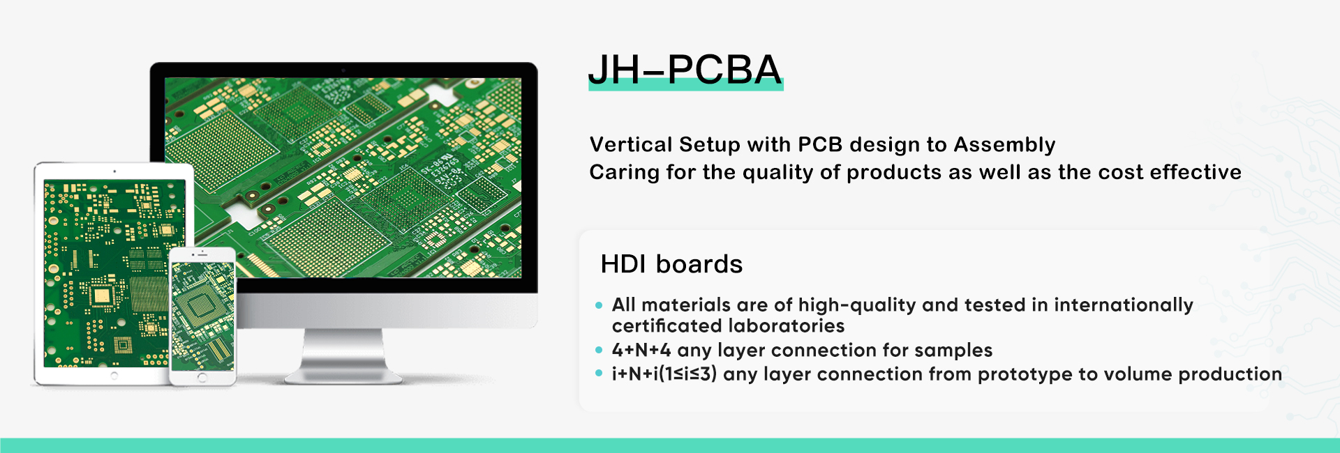
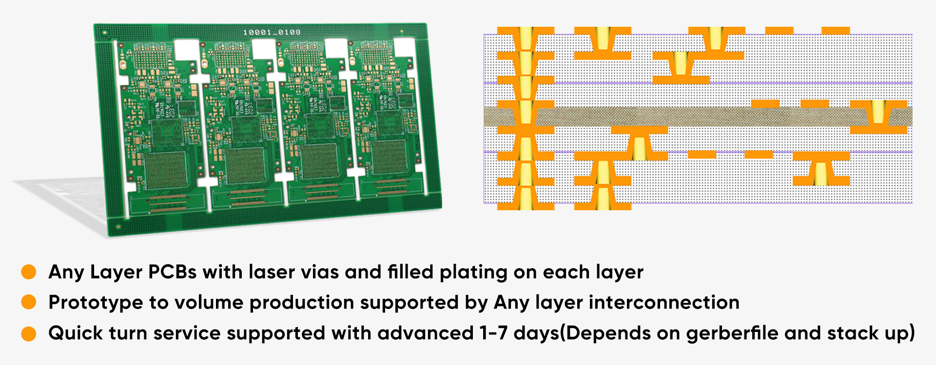
HDI stands for High Density Interconnect PCB. Due to their increased density, they provide an essential routing solution for the large pin-count chips used in mobile devices and other high-tech products.
What type of HDI boards can you get from us?
Due to design constraints, HDI PCBs have much higher routing and pad connection densities than conventional PCBs. The structure construction is explained below.
1+N+1– The PCB contains 1 High Density Interconnect layer "build".
i+N+i (i≥2)– The PCB contains 2 or more "build-up" high-density interconnect layers. Microwells on different layers can be staggered or stacked.
Any layer HDI– The layers of the PCB are high-density interconnect layers that allow conductors on any layer of the PCB to freely interconnect with copper-filled stacked microvia structures.
Applications of HDI PCBs:
·Automobile industry:Engine control unit, GPS, dashboard electronics.
·Telecommunications Industry:Computers, Laptops, Tablets, Wearable Electronics, IoT
·army:Military routers, COTS boards, etc.
· medical:35 micron microspace plate, pacemaker
· Semiconductor:MCM/Flip Chip/Wire Bond, Stacked Micro Via
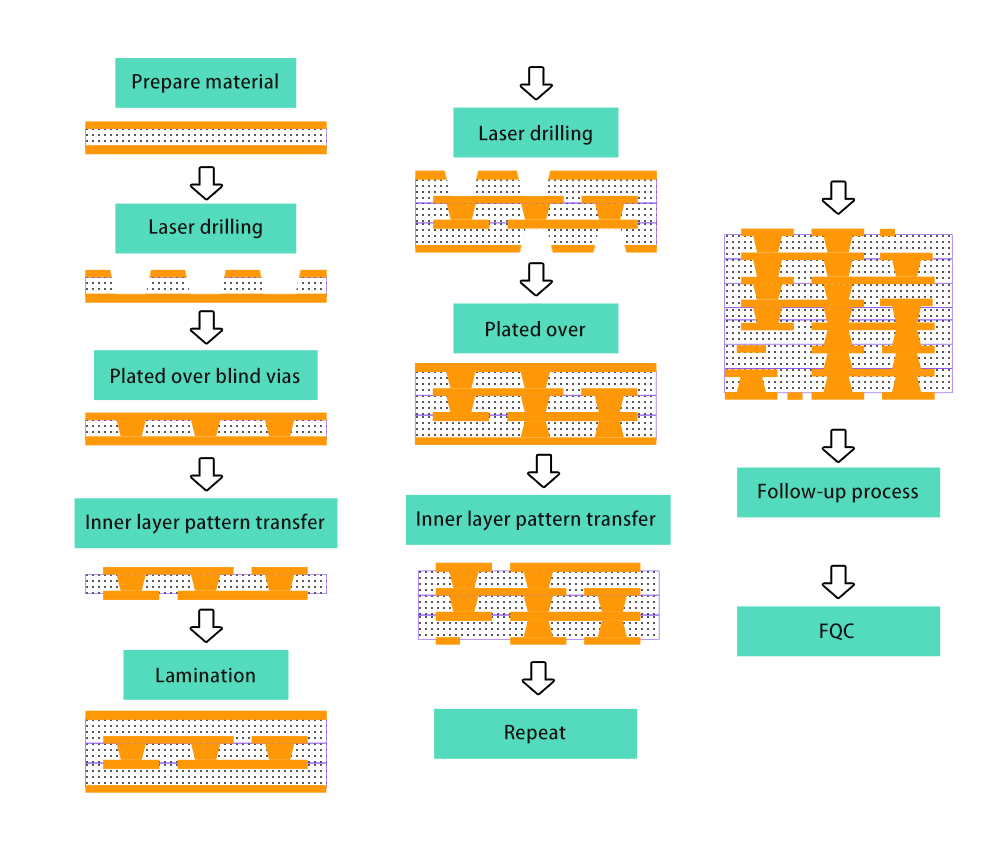
HDI production process:
| HDI PCB process capability | ||
| project | content | production capacity |
| 1 | layers | Standard 4-22 layers, advanced 30 layers |
| 2 | Material | FR4 Standard, FR4 High Performance, Halogen Free FR4, Rogers |
| 3 | Copper products | 18um-70um |
| 4 | Minimum tracks and clearances | 0.075mm/0.075mm |
| 5 | PCB thickness | 0.4mm-6.0mm |
| 6 | biggest size | 610mm*450mm, depends on the laser drilling machine |
| 7 | surface treatment | OSP, ENIG, immersion tin, immersion silver, electrolytic gold, gold finger |
| 8 | minute. mechanical drill | 0.15 mm |
| 9 | minute. laser drilling | Standard 0.1mm, Advanced 0.075mm |
| 10 | Quality Standard | IPC-600, 6012, Class II & III |
| 11 | HDI | 4+N+4, 4-step arbitrary layer connection |
-
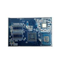
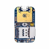
UA65KS8800JXXZ motherboard BN41-02504A

-
Custom Logo China Ems Oem Custom Electronic Circuit Board Supplier Inverter Charger Pcb
-
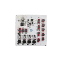
daly bms 48v 16s placa de circuito maker mppt board 24s bms parallel bms hf driver pcb assembly
-
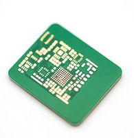
Finished product inspection pcb production gerber circuit board pcb board design
-
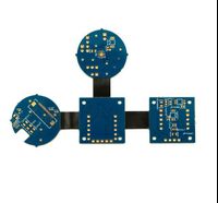
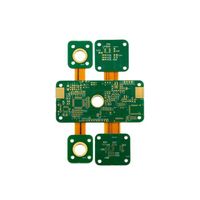
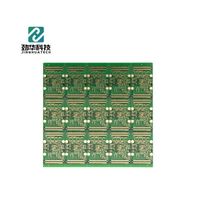
HDI PCB immersion gold printed circuit board ENIG PCBA assembly blind hole pcb
-
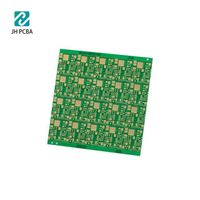
JINHUA brand manufacturer FR4 1.6mm HDI high density pcb interconnect board
-
Professional OEM HDI PCB Circuit Board For Sports Watch Boards Factory Direct Sales
-
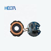
GPS locator PCB circuit board PCBA belt project development service
-
bin sensor pcb 24s smart deligreen bms drone board daly 200a 4s gps tracker pcb jk bms 4s 3s bms
-
JINHUA PCB serves Immersion Gold Multilayer PCB with high density PCB
Other Products
-
$0.10 - $3.90 / piece
-
$0.10 - $3.50 / piece
-
$0.10 - $3.90 / piece
-
$0.10 - $3.90 / piece
-
$0.10 - $3.50 / piece
-
$0.10 - $3.50 / piece
-
$0.10 - $3.90 / piece
-
$0.10 - $3.50 / piece
-
$0.10 - $3.50 / piece
-
$0.10 - $3.50 / piece