- Products
- Products
- Companies
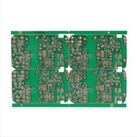
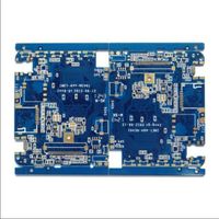
USB interface PCB schematic layout engineer design service

-
Supplier: Shenzhen City Yueda Technology Co., Ltd. -
Region: Guangdong, China -
Contact: Ms Christine Qiu -
Price: $0.35 / 2 - 99 pieces
$0.20 / 100 - 999 pieces
$0.10 / >=1000 pieces -
Min. Order: 2 pieces
Product details
| brand: | PCB design service | Material: | FR4/Aluminum/Ceramic CEM1 |
| Substrate: | FR-4 glass epoxy | Packaging Details: | Bubble bag inside, international standard carton outside |
| Copper thickness: | 0.5 oz - 6.0 oz | minute. line width: | 3 million |
| pack: | vacuum packaging | Layers: | 1-32 liters |
| MOQ: | 1 | minute. Hole size: | 6mil, 4mil-laser drill |
| model: | YD-D032 | payment terms: | L/C, T/T |
| Origin: | Guangdong, China | PCB standard: | IPC-A-610D/IPC-III standard |
| Plate thickness: | 1.6 mm | PCBA service: | SMT DIP parts assembly |
| Surface treatment: | tin, nickel | port: | Shenzhen |
| minute. Line spacing: | 3 million | color: | red blue green black white |
| Supply capacity: | 500000 pieces per month | product name: | Custom soft and hard PCB |
| Board size: | Maximum 600 X 1200MM | application: | Large, medium and small projects |
| Serve: | Provide OEM service |
Product Description
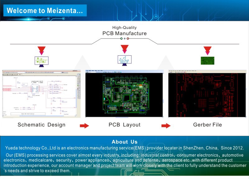
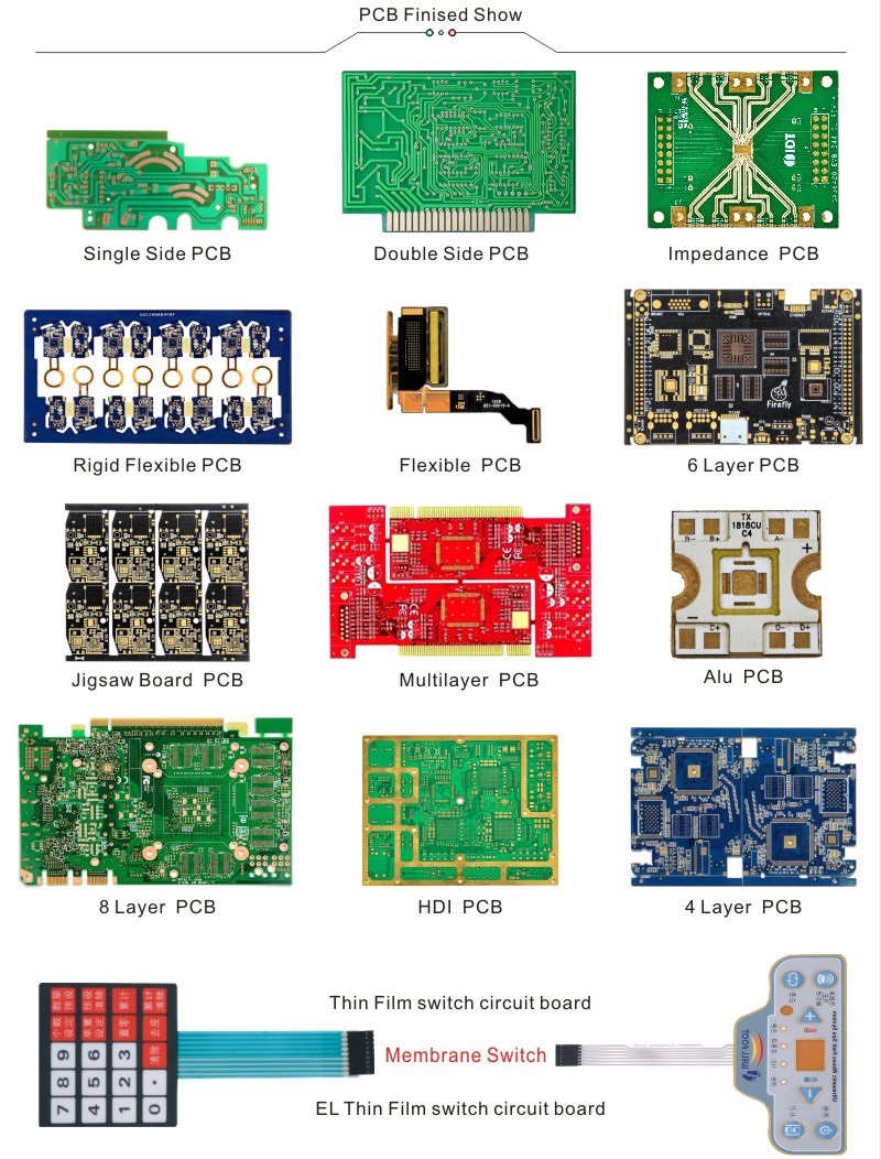
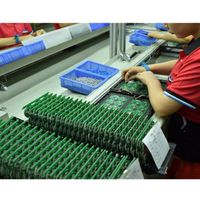
 Printed Circuit Board Manufacturing
| No. | thing | Specification |
| PCB Manufacturing Capability | ||
| 1 | PCB layers | 1 to 32 floors |
| 2 | PCB board material type | CEM-1, FR4, High TG FR4, ALU, CEM-3, Rogers, HDI, etc. |
| 3 | biggest size | 600×1200 mm |
| 4 | Minimum Line Width | 0.1mm |
| 5 | Minimum spacing | 0.1mm |
| 6 | Dimensional tolerance | ±0.1 mm |
| 7 | minimum aperture | 0.2mm |
| 8 | PCB board thickness coverage | 0.2 to 6.0mm |
| 9 | Minimum copper thickness in the hole | 0.02mm |
| 10 | DK thickness | 0.08 to 6.0 mm |
| 11 | NPTH Dimensional Tolerance | ±0.025mm |
| 12 | Plated Through Hole Dimensional Tolerance | ±0.025mm |
| 13 | Dimensional tolerance | ±0.1mm |
| 14 | Hole tolerance | 0.075 mm |
| 15 | Laser drilling size | 0.1mm |
| 16 | Minimal Sun Mask | 0.01mm |
| number 17 | Minimum Dimensions of Solder Mask Spacer Ring | 0.05 mm |
| 18 | Maximum plate twist and wrap | ≤1% |
| 19 | Finished aperture | 0.2 to 6.0 mm |
| 20 | flame retardant | 94V-0 |
| twenty one | Impedance Control Tolerance | ±5% |
| twenty two | Outer copper thickness | 8.75 to 175 microns |
| twenty three | Inner layer copper thickness | 17.5 to 175 microns |
| twenty four | Solder mask type | blue, green, black, yellow, red, white |
| 25 | surface finish | Immersion gold, gold plating, immersion silver, immersion tin, etc. |
| 26 | Certificate | ISO9001, ISO14001, ISO14969 |
Production Process

our service

Capabilities and scope of services:
♦PCB circuit layout and production
❖Plastic and Metal Housing Design Service
❖Customized product packaging design
♦SMT/SMD parts assembly and diP through-hole soldering (PCBA)
♦IC programming software (pre-programming), PCBA function test and verification
Complete product assembly (including plastic, metal casing, PCBA main board, cables, switches and other components, etc.)
♦RoHS environmental protection material supply
❖ Logistics arrangements, import and export of goods from China

Packaging and Shipping

VIEW MORE
You may like
-
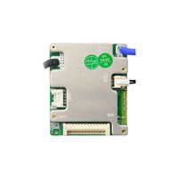
Jiabaida built-in BT BMS 7s 8s 10s 12s 13s 14s 24V 36V 48V 20A 30A automatically identifies BMS with UART NTC

-
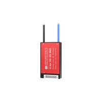
Daly bms manufacturer pcb oem electric vehicle ev Lithium LI-ION 18650 Battery Pack 10S 36V 15A 20A BMS management system
-
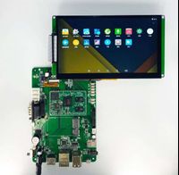
Development board with LCD touch screen lcd lvds GPIO development board with Ethernet and USB interface driver board
-
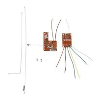
4 Channel Remote Control 27MHz Circuit PCB Transmitter and Receiver Board with Antenna Radio System for Car Truck Toys
-
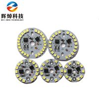
China Electronics PCB/PCBA Supplier LED PCB Board Light
-
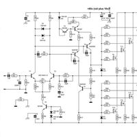
Schematic diagram of electronic circuit diagram of mobile power pcb board
-
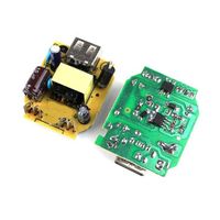
R&D USB Charger PCBA Power Adapter PCB Assembly Smartphone Accessories Electronics Manufacturer
-
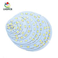
High Quality 9W High Voltage SMD 2835 AC220V LED Printing Round Paint LED Aluminum PCB for Tube Light
-
Custom BGA PCBA Supplier Professional Circuit Board Assembly Manufacturer PCB PCBA Fabrication Service Factory
-
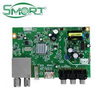
Smart Electronics~DVB T2 ISDB-T ATSC pcb set top box high quality
Other Products
-
$0.10 / piece
-
$0.10 / piece