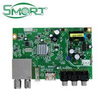
- Products
- Products
- Companies
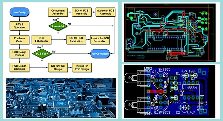
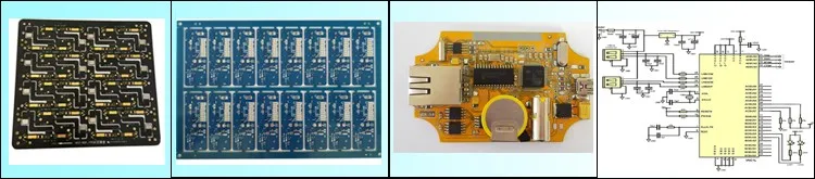
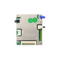
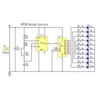
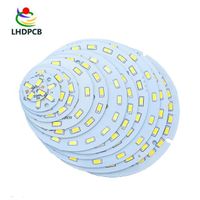
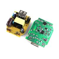
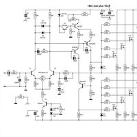
Schematic diagram of electronic circuit diagram of mobile power pcb board

-
Supplier: Gesp Technology (Dalian) Co., Ltd. -
Region: Liaoning, China -
Contact: Ms Miki Liu -
Price: $2.00 /piece -
Min. Order: 1 piece
Product details
| Copper thickness: | 0.25 oz - 12 oz | standard: | IPC Class 2, Class 3 |
| Printed Circuit Board Project: | Schematic diagram of electronic circuit diagram of mobile power pcb board | Minute line width: | 0.1 mm |
| Solder Mask: | Green/Blue/Black/Red/Yellow/White | Surface treatment: | HASL lead-free/OSP/soft gold/hard gold, HASL\OSP\DOLD Finger\ENIG\Solder Mask\tinned |
| application: | Electronic equipment | Origin: | Guangdong, China |
| Controlled Impedance Tolerance: | yes or no according to gerber file | Substrate: | FR-4/aluminum/ceramic/cem-3/FR-1,FR-4/aluminum/ceramic/cem-3/FR-1 |
| Packaging Details: | Schematic diagram of electronic circuit diagram of mobile power pcb board Packaging details: inner packing: vacuum bag outer packing: carton | port: | Shenzhen, Dalian, Hong Kong |
| brand: | Gap | Supply capacity: | 8000 square meters per month |
| Testing service: | Electronic test or flying probe test according to the order quantity | payment terms: | L/C, Western Union, D/P, D/A, T/T, paypal |
| Plate thickness: | 0.005"-0.250" | Blind buried via: | yes or no according to gerber file |
| Minute Hole Size: | 0.20mm | Minute line spacing: | 0.1 mm |
| model: | PCB Assembly | Certificate: | ISO/RoHS/TS16949 |
Schematic diagram of electronic circuit diagram of mobile power pcb board
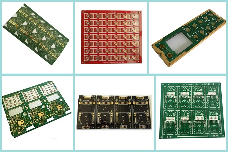
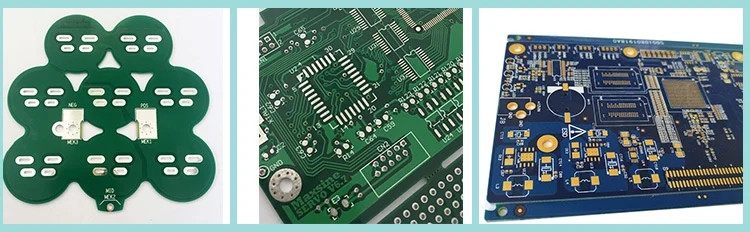
Product Description

Our main product strength
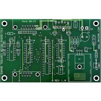
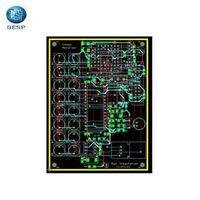
No.1 PCB Design and Layout Services
No.2 double-sided PCB
No.3 Multilayer PCB 4 to 40 layers
No.4 PCB assembly
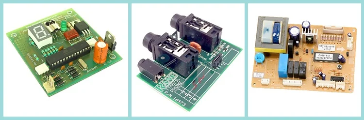
other products
Europer The main business is PCB manufacturing, PCB replication and PCB design, such asWashing machine pcb board, air conditioner frequency conversion pcb board, mobile phone pcb board, mobile power supply pcb, etc.other products:
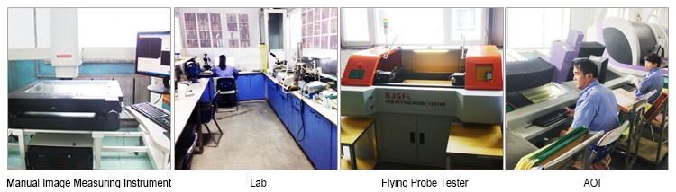
Circuit board equipment

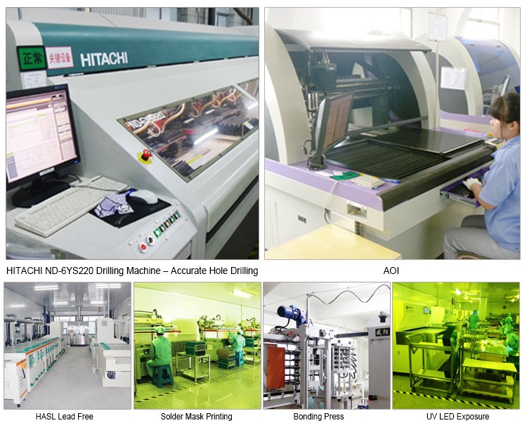
PCB testing equipment.
VIEW MORE
You may like
-
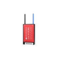
Jiabaida built-in BT BMS 7s 8s 10s 12s 13s 14s 24V 36V 48V 20A 30A automatically identifies BMS with UART NTC

-
Daly bms manufacturer pcb oem electric vehicle ev Lithium LI-ION 18650 Battery Pack 10S 36V 15A 20A BMS management system
-
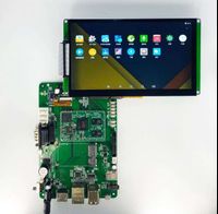
Development board with LCD touch screen lcd lvds GPIO development board with Ethernet and USB interface driver board
-
USB interface PCB schematic layout engineer design service
-
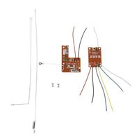
4 Channel Remote Control 27MHz Circuit PCB Transmitter and Receiver Board with Antenna Radio System for Car Truck Toys
-
China Electronics PCB/PCBA Supplier LED PCB Board Light
-
R&D USB Charger PCBA Power Adapter PCB Assembly Smartphone Accessories Electronics Manufacturer
-
High Quality 9W High Voltage SMD 2835 AC220V LED Printing Round Paint LED Aluminum PCB for Tube Light
-
Custom BGA PCBA Supplier Professional Circuit Board Assembly Manufacturer PCB PCBA Fabrication Service Factory
-
Smart Electronics~DVB T2 ISDB-T ATSC pcb set top box high quality
Other Products
-
$5.00 / piece
-
$2.00 / piece
-
$0.10 / piece
-
$0.01 / unit
Related Search
design of electronic circuits
types of mobile cranes
lowest price of mobile in china suppliers
manufacturers of mobile suppliers
fast electron circuit suppliers
electronic circuit modules suppliers
infrar electron circuit suppliers
electronics circuit board
mobile phone pcb circuit board suppliers
oem design electronic circuits suppliers