- Products
- Products
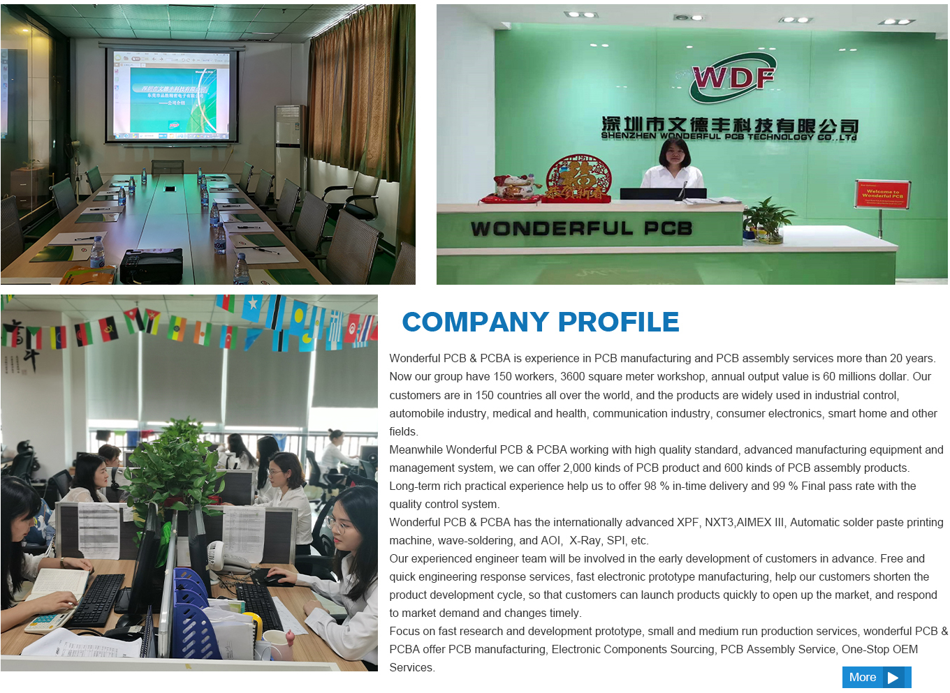
- Companies
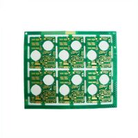
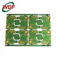
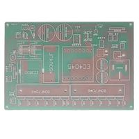
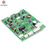
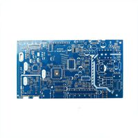
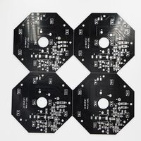
PCB Reverse Engineering Gerber Cloning and BOM Clone Service

-
Supplier: Shenzhen Wonderful Technology Co., Ltd. -
Region: Guangdong, China -
Contact: Ms Miss Gong -
Price: $0.50 /piece -
Min. Order: 1 piece
Product details
| Packaging Details: | Gerber and BOM clone service inner packing: vacuum packing/polybag; outer packing: standard carton packing. | brand: | Wonderful PCB |
| Minute Aperture: | 0.1mm | test: | 100% electronic test; functional test |
| Certificate: | rose. ISO9001 | port: | Shenzhen, Hong Kong |
| Keyword two: | Gerber clone | other service: | Complete product assembly, IC programming, component procurement |
| Solder mask color: | Green, black, blue, yellow, red, etc. | model: | PCB reverse engineering |
| product name: | PCB Reverse Engineering China | Board Dimensions: | OEM production |
| Silkscreen: | White, yellow, red, blue, etc. | Supply capacity: | 40000 square meters per month |
| Origin: | Guangdong, China | Keyword three: | PCBA Gerber and BOM Clone Services |
| Keyword one: | PCB reverse engineering | Copper thickness: | 2 oz |
| Substrate: | FR-4 | Minute line width: | 0.1 mm |
| payment terms: | L/C, Western Union, D/P, D/A, T/T, MoneyGram, Paypal | type: | Electronics, smart home, ultrasonic sensor, single-sided pcb |
| Surface treatment: | HASL | Plate thickness: | 1.6 mm |
| Minute line spacing: | 0.1 mm |
One-stop OEM service
If required, we will source, organize and manage all aspects of PCB design so that your product meets all required standards and is fully optimized for simple and cost-effective manufacturing. A well-designed board means: · Fewer production problems · Improved quality control · Reduced costs · Reduced manufacturing timeWe are committed to providing our customers with competitively priced printed circuit boards in both small and large quantities.
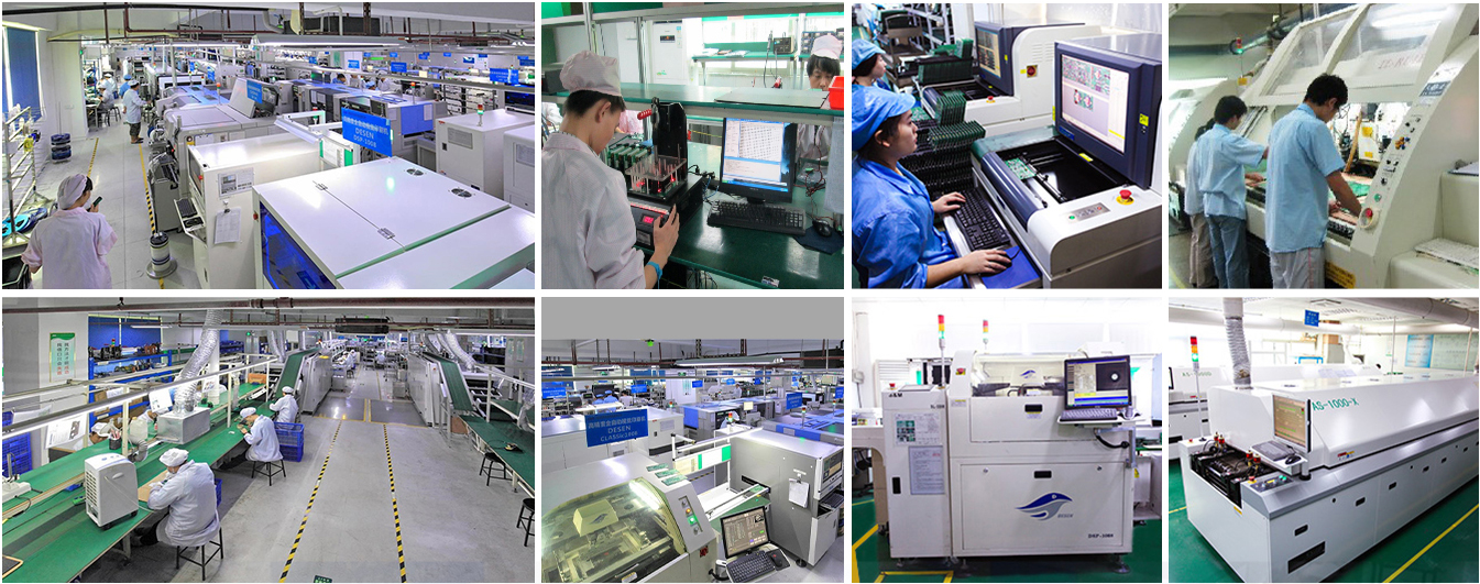
PCB&PCBA capacity building
PCB capability | ||||||||
layers | 1 - 20 floors | |||||||
Maximum processing area | 680×1000MM | |||||||
Minimum plate thickness | 2 layers - 0.3MM (12 million) | |||||||
4 layers - 0.4MM (16 million) | ||||||||
6 layers - 0.8MM (32 million) | ||||||||
8 layers - 1.0MM (40 million) | ||||||||
10 layers - 1.1MM (44 million) | ||||||||
12 layers - 1.3MM (52 million) | ||||||||
14 layers - 1.5MM (59 million) | ||||||||
16 layers - 160 mm (63 million) | ||||||||
18 layers - 1.8MM (71 million) | ||||||||
Finished plate thickness tolerance | Thickness≤1.0MM, tolerance: ±0.1MM | |||||||
1.0MM≤thickness≤6.5MM, tolerance ±10% | ||||||||
twist and bend | ≤ 0.75%, min: 0.5% | |||||||
TG range | 130 - 215°C | |||||||
Impedance tolerance | ± 10%, minimum: ± 5% | |||||||
Pressure test | Maximum value: 4000V/10MA/60S | |||||||
surface treatment | HASL, leaded, HASL lead-free | |||||||
Flash gold, heavy gold | ||||||||
sinking silver, sinking tin | ||||||||
Golden Finger, OSP | ||||||||
PCB assembly capability | PCB assembly capability | |||||||
quantity of order | 1 piece – over 10,000,000 pieces | |||||||
build time | 1 – 5 days, 1 – 2 weeks or scheduled delivery | |||||||
PCB specification requirements | PCBs with width/length less than 30mm should be assembled Maximum board size: 500×450 mm Circuit board type: rigid PCB, flexible PCB, metal core PCB Surface treatment: lead/lead-free HASL, ENIG, silver, OSP | |||||||
Assembly type | surface mount Throat hole Mixed technology (SMT and through-hole) Single or double sided placement Conformal Coating Shield Assemblies for EMI Emissions Control | |||||||
Solder type | Lead-free – RoHS | |||||||
Parts procurement | full turnkey part turnkey Complete set/consignment | |||||||
component type | SMT 01005 or larger BGA 0.4mm pitch, POP (package on package) WLCSP 0.35mm pitch Hard Metric Connectors Wire and Cable | |||||||
Introduction of SMT Parts | most cutting tape part scroll reel tube tray | |||||||
template | Laser cut stainless steel | |||||||
other technologies | Free DFM Review box assembly BGA 100% AOI test and X-ray test IC programming Component costs drop custom function test protection technology | |||||||


Finding the best supplier for PCBs can be a challenge - meeting each and every customer's expectations and requirements for price, quality, lead time, value-added services and delivery.Wonderful PCBWe are sure we meet your every expectation with every PCB.
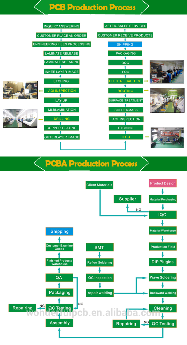
Production Process
about Us
contact us

VIEW MORE
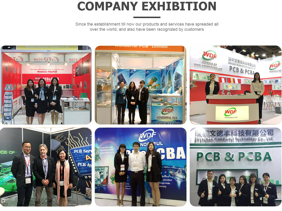
You may like
-
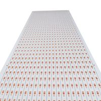
Various printed single-sided PCB vacuum circuit board customization services

-
Hot Selling Fr4 Single Sided Green PCB Printed Circuit Board Customized PCBA Assembly Prototype Service OEM ODM Factory
-
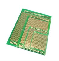
Green printed circuit board 6X8/10X15/12X18cm single-sided PC board 2.54mm PCB universal board DIY experimental breadboard
-
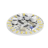
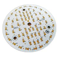
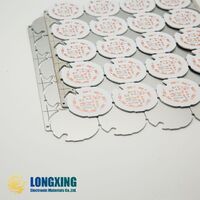
Printed Circuit Board Blank Pcb Round Size Square Size mcpcb Size For 3w 5w 7w 9w 12w 15w 18w Led Bulb
-
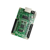
OEM PCB IoT PCB Assembly
-
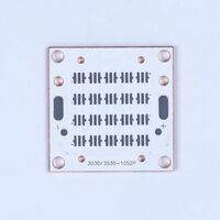
120cm 150cm LED Tube Metal Pcb Strip Mcpcb Board 5730 SMT Single Layer Side Aluminum Circuit Board T6 T8 LED Tube
-
mcpcb 94v-0 pcb copper metal core direct thermal path pcb board pcba manufacturer for led light
-
Custom Electronic Circuit Board Assembly PCBA Manufacturer Single Sided PCB
-
High quality high power single layer aluminum round shape led pcb 220v, MCPCB , pcb board
-
Single Layer Printed Circuit Board Single Sided Pcb Used For Automotive Lighting Car Light
Other Products
-
$0.10 / piece
-
$0.35 / piece
-
$0.10 / piece
-
$0.10 / piece
-
$2.90 / piece
-
$0.30 / piece