- Products
- Products
- Companies
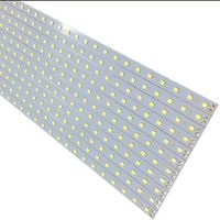
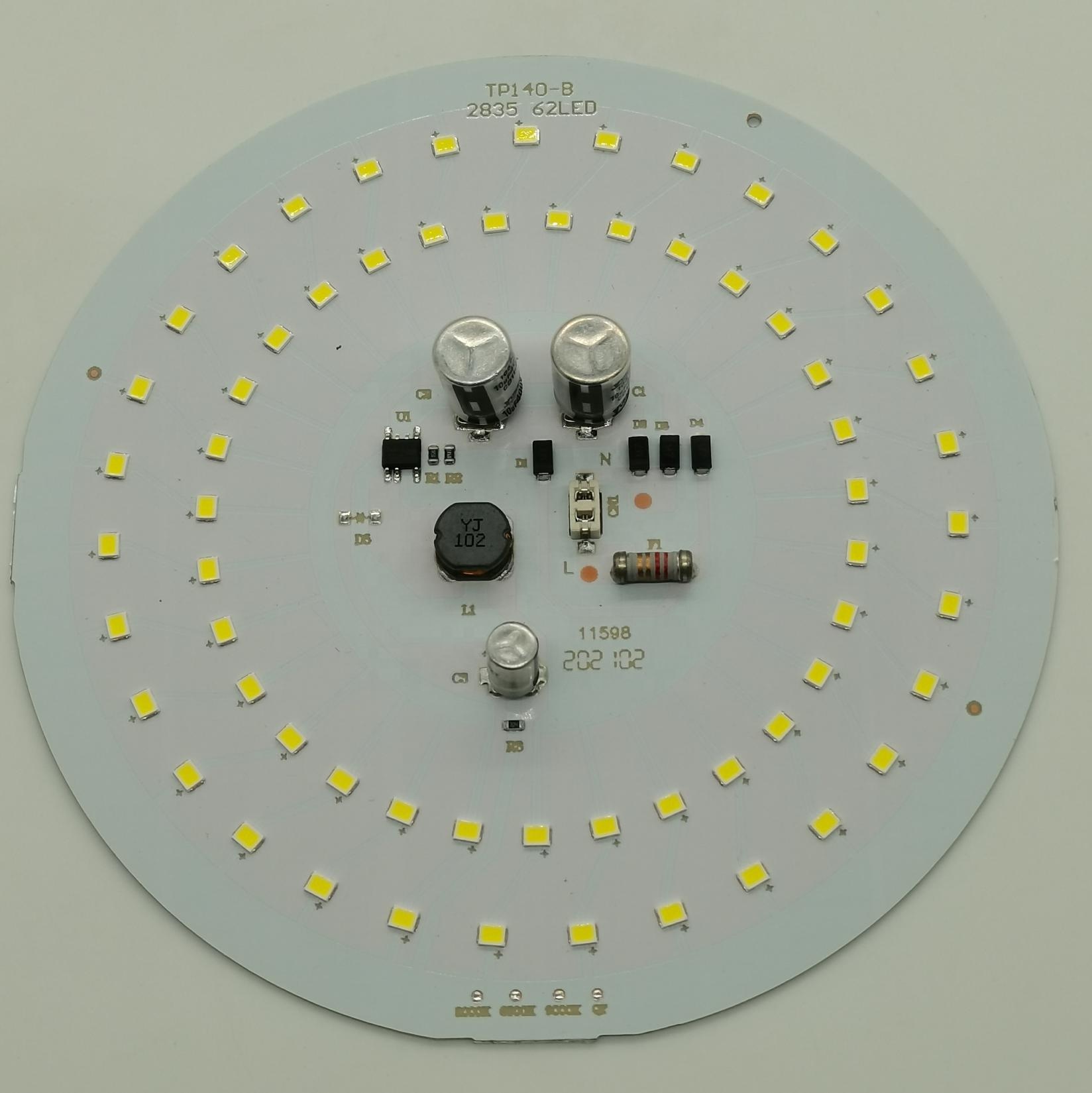
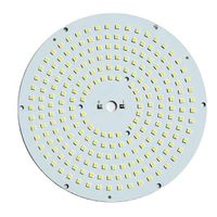
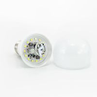
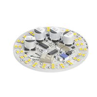
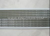
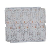
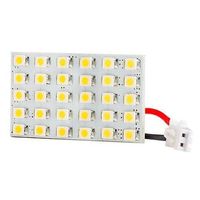
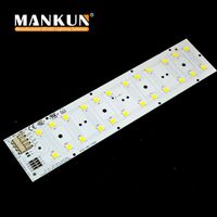
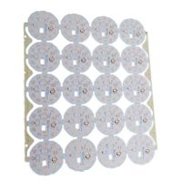
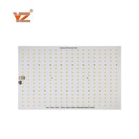
Bulb lamp pcba design chip patch led PCB bulb lamp circuit board

-
Supplier: Jiangmen Xinda Electronic Co., Ltd. -
Region: Guangdong, China -
Contact: Ms Serena Zhan -
Price: $0.50 / 1 - 4999 pieces
$0.40 / >=5000 pieces -
Min. Order: 1 piece
Product details
| Surface treatment: | Immersion tin, OSP | Packaging Details: | PE film packaging, vacuum packaging machine, carton |
| application: | LED lighting | Production capacity: | 500,000 square meters/month |
| Solder Mask: | green. Red. blue. white. Black. Yellow | MOQ: | 1 |
| Minute line spacing: | 0.15mm | Package preview: | |
| Plate thickness: | 0.4/0.6/0.8/1.0/1.2/1.5/1.6/2.0/3.0mm | place of origin; place of origin: | Guangdong, China |
| Minute line width: | 0.15mm | model: | XD-SMD-3 |
| port: | Zhongshan Port, Shenzhen Port, Guangzhou Port | type: | Aluminum plate |
| printing art: | screen printing | Board Dimensions: | 0.4/0.6/0.8/1.0/1.2/1.5/1.6/2.0/3.0mm |
| layer: | single layer | Supply capacity: | 1,000,000 pieces per month |
| Copper thickness: | 15uf, 18uf, 22uf, 25uf, 35uf, etc. (1/2oz-2oz) | Serve: | One-stop service |
| brand: | Xinda | payment terms: | Western Union, T/T |
| Substrate: | FR4,FPC, CEM-3, 22F, VO, HB, KB | Minute Hole Size: | Single layer, 0.5mm |
| LED light source: | 3000K/4000K/6000K etc. |
Product Description
Bulb lamp pcba design chip patch led PCB bulb lamp circuit board

thing | Processing capacity |
raw material | Various thickness PCB boards, FR4, FPC, CEM-3, 22F, VO, HB, KB |
printing art | screen printing |
surface treatment | HASL(LF), Gold Plated, Enig, Immersion Gold, Immersion Tin, OSP |
layers | single layer |
metal base type | Copper base, aluminum base, glass fiber |
metal thickness | 0.4/0.6/0.8/1.0/1.2/1.5/1.6/2.0/3.0mm |
Solder Mask and Silkscreen Colors | Green/Black/White/Red/Blue/Yellow |
Thermal Conductivity | Normal 0.5W, Medium 1.0W, High 1.5W |
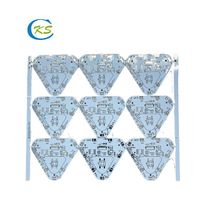
Plate shape | Rectangular, round, grooved, notched, complex and irregular |


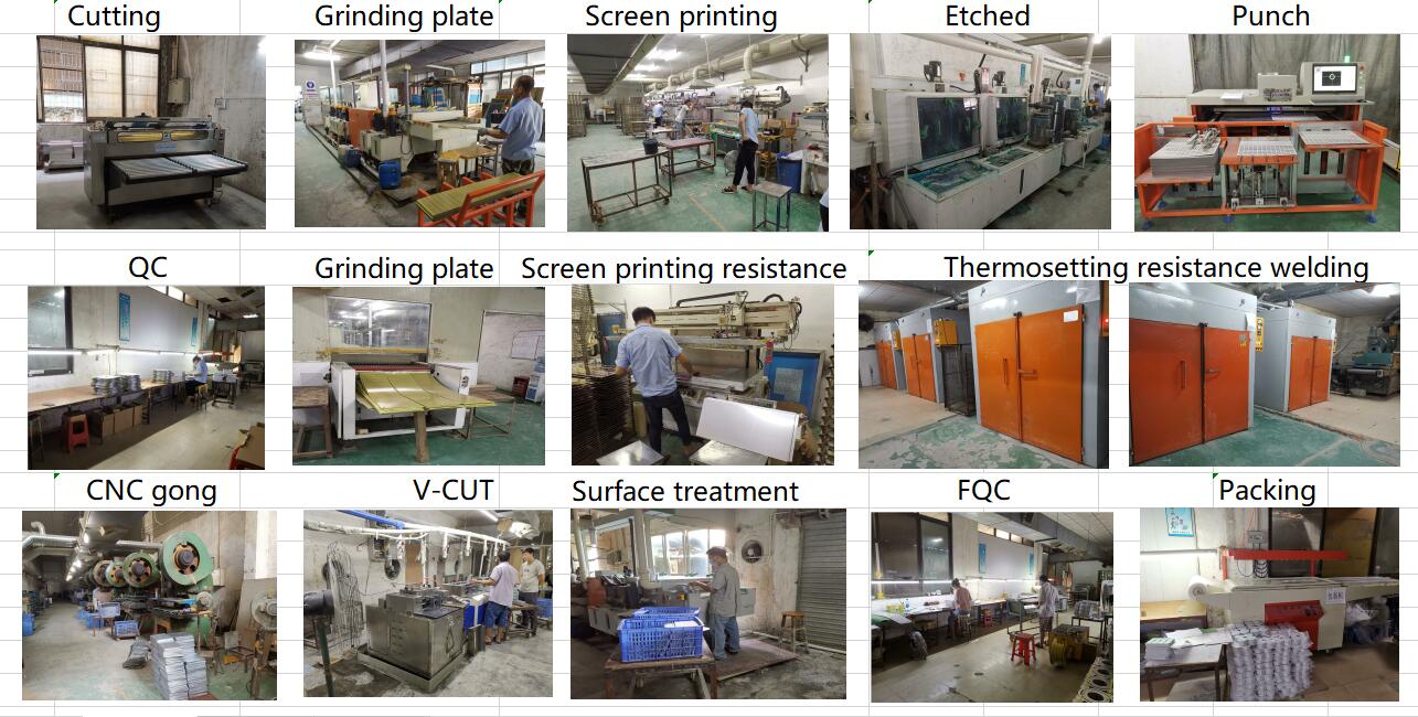
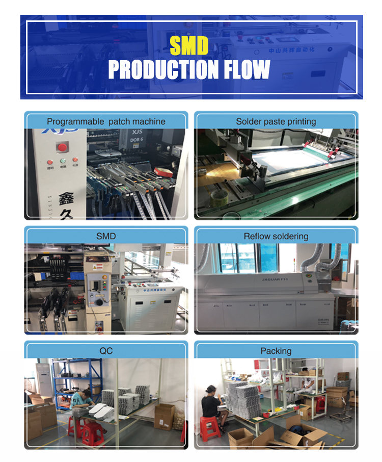
Manufacturing Technology
Aluminum LED PCB production process
Chip production process
VIEW MORE
You may like
-
China 94v0 LED PCB manufacturing PCBA prototype cheap price LED led pcba panel SMD light circuit PCB

-
Customized 9w 12w 15w 18w Led light bulb PCB round panel assembly 12v 24v SMD 5050 5730 2835 5630 LED PCBA aluminum base circuit board
-
China Reliable and Custom PCB Supplier with high quality electronic pcb aluminum plate
-
Professional Chinese OEM Manufacturing PCB PCB Board PCB 94v0 LED Aluminum PCB
-
2Layers Aluminum Core PCB
-
LED Pcb Manufacturing Lamp Accessories Mcpcb Board Aluminum Pcb Board
-
Best Selling 30w-50w Aluminum Micro SMD LED Light PCB Board
-
SMD5050 7700 lm aluminum plate flood tunnel light street light led module pcb
-
China Aluminum LED Bulb PCB, SMD LED Custom PCB OEM ODM Circuit Board For DOB Bulb
-
Samsung LM301H 301B plant light assembly pcb with LED PCB module circuit board plant light PCBA
Other Products
-
$0.10 - $0.50 / piece