- Products
- Products
- Companies
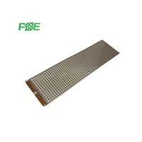
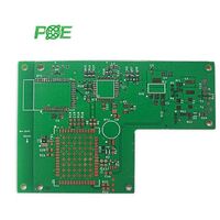
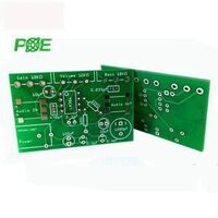
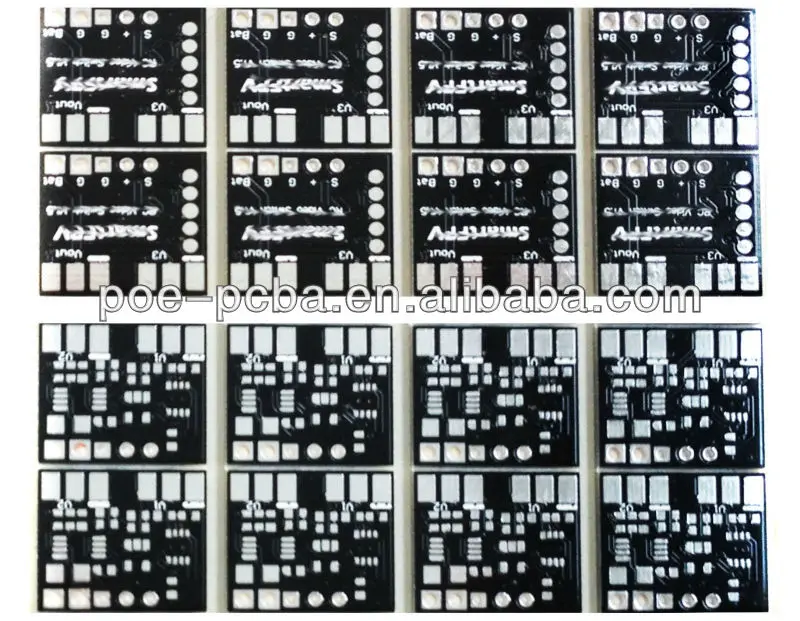
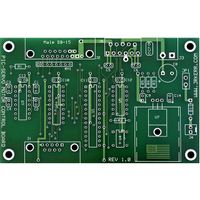
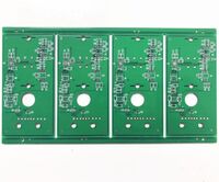
2 Layer Micro SD Card PCB

-
Supplier: Shenzhen POE Precision Technology Co., Ltd. -
Region: Guangdong, China -
Contact: Ms Vicky Liang -
Price: $1.00 /piece -
Min. Order: 1 piece
| Finised copper thickness: | 1-6OZ; | Model Number: | PCB-5359; |
| Payment Terms: | L/C,T/T,Western Union,Micro SD Card PCB; | Solder Mask Color: | Green\White\Red\Blue\Black; |
| Layers: | 1-28; | Min. Line Width: | 0.1mm; |
| Supply Ability: | 30000.0 Square Meter/Square Meters per Month Micro SD Card PCB; | Impedence Control Tolerance: | ±5%; |
| Brand Name: | POE; | Place of Origin: | Guangdong China; |
| China: | Micro SD Card PCB; | PCB Standard: | IPC-A-610 D; |
| Finished board thickness: | 0.2-7.0mm; | Port: | Shenzhen; |
| Board Size: | Optional; | Min. Hole Size: | 0.2mm; |
| Surface Finishing: | HASL lead free; | OEM/ ODM Service: | One-stop turnkey Service; |
| Copper Thickness: | 1oz; | Color: | Green,Blue,Black,Red,Yellow,white; |
| Min. Line Spacing: | 0.1mm; | Packaging Detail: | CNC package for bare PCB and ESD package for PCBA assemble with POE box Package; |
| Base Material: | FR4; | Hole tolerance: | PTH: ±3mil, NTPH: ±2mil; |
| Board Thickness: | 1.6mm; |
China Micro SD Card PCB
|
1.High quality micro SD card pcb 2.2 Layer HASL lead free SD pcb 3.Double sided black solder mask pcb 4.100%E-test before shipment 5.One-stop turnkey service 6.Small order is acceptable |
|
WELCOME TO POE
We are able to provide you best electronics services.
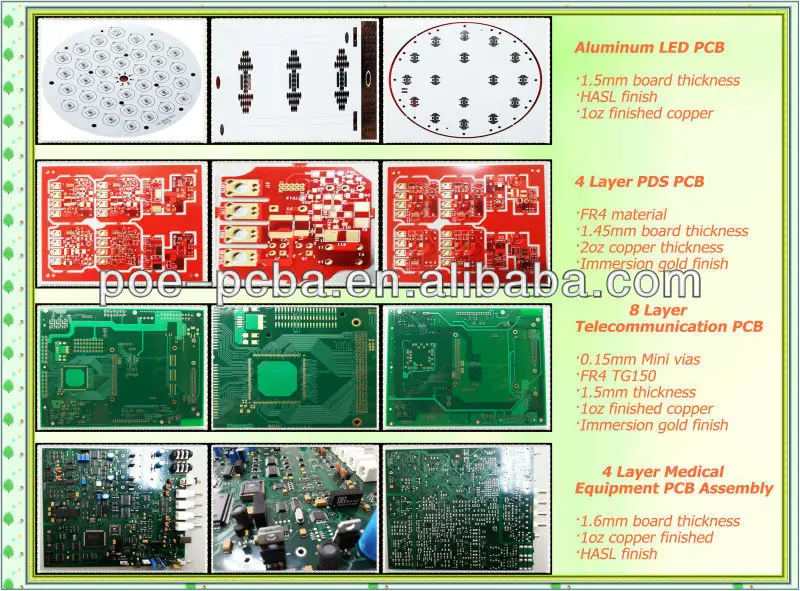
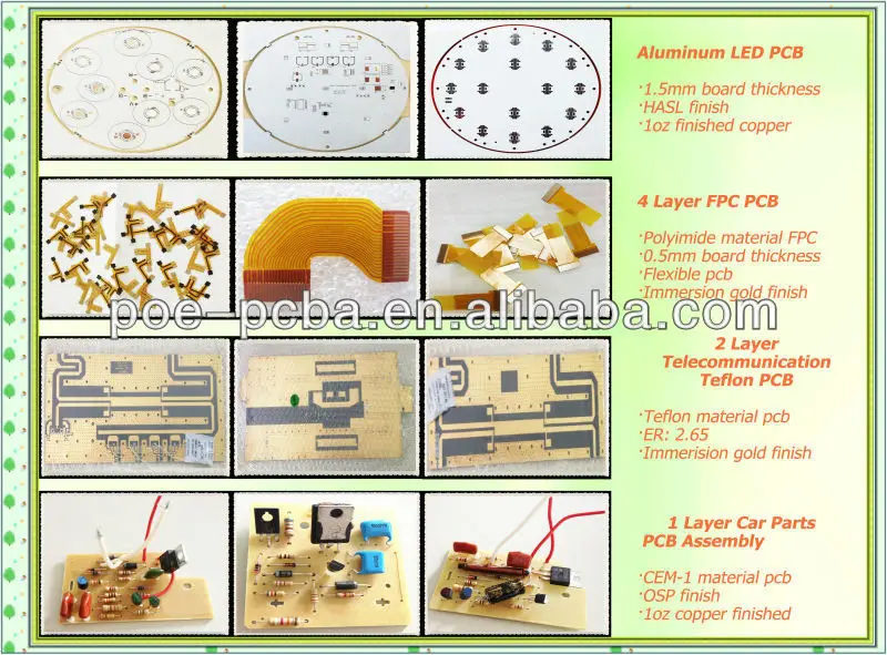
- PCB Production Service. (FR-4,HI-TG,Aluminum,FPC,TEFLON,CEM-1 )
- FPC,PCB Copy Service.
- PCB Assembly Service. (SMT, BGA, DIP)
- PCBA Housing assembly serivce.
- PCBA Final Functional Testing
- PCBA Copy Service.
- Electronic Components Purchasing & BOM List Purchasing Services.
- PCB SMT Stencil. (Laser cut & Etching)
1. POE PCB Manufacture Capability
|
Item |
Capability |
|
|
1.Base Material |
FR-4 / High TG FR-4 / Lead free Materials (ROHS Compliant) / Halogen Free material /CEM-3/CEM-1/ /PTFE/ROGERS/ARLON/TACONIC |
|
|
2.Layers |
1-28 |
|
|
3.Finised inner/outer copper thickness |
1-6OZ |
|
|
4.Finished board thickness |
0.2-7.0mm |
|
|
Tolerance |
Board thickness≤1.0mm: +/-0.1mm 1 Board thickness>2.0mm: +/-8% |
|
|
5.Max panel size |
≤2sidesPCB: 600*1500mm Multilayer PCB: 500*1200mm |
|
|
6.Min conductor line width/spacing |
Inner layers: ≥3/3mil Outer layers: ≥3.5/3.5mil |
|
|
7.Min hole size |
Mechanical hole: 0.15mm Laser hole: 0.1mm |
|
|
Drilling precision: first drilling |
First drilling: 1mil Second drilling: 4mil |
|
|
8.Warpage |
Board thickness≤0.79mm: β≤1.0% 0.80≤Board thickness≤2.4mm: β≤0.7% Board thickness≥2.5mm: β≤0.5% |
|
|
9.Controlled Impedance |
+/-5% |
|
|
10. Aspect Ratio |
15:1 |
|
|
11.Min welding ring |
4mil |
|
|
12.Min solder mask bridge |
≥0.08mm |
|
|
13.Plugging vias capability |
0.2-0.8mm |
|
|
14. Hole tolerance |
PTH: +/-3mil NPTH: +/-2mil |
|
|
15.Outline profile |
Rout/ V-cut/ Bridge/ Stamp hole |
|
|
16.Surface treatment |
OSP: 0.5-0.5um HASL: 2-40um Lead free HASL: 2-40um ENIG: Au 1-10U’’ ENEPIG: PB 2-5U’’/ Au 1-8U’’ Immersion Tin:0.8-1.2um Immersion silver: 0.1-1.2um Peelable blue mask Carbon ink Gold plating: Au 1-150U’’ |
|
|
17. E-testing pass percent |
97% pass for the first time,+/-2%(tolerance) |
|
|
FQC-Physical Lab: Reliability tests |
||
|
18.Certificate |
ROHS E327776 ISO9001:2008 IPC SGS |
|
|
|
||
|
Our equipments |
||
|
1.Drilling workshop |
4 drilling bits of drilling machine: 4 sets 2 drilling bits of drilling machine: 2 sets |
|
|
2. photo plotting workshop |
Israel “ORBOTECH” Photo Plotters |
|
|
3.AOI |
AOI machine |
|
|
4.IPQC |
“OXFORD” CMI 700 Copper Thickness Tester |
|
|
5.Impedance test |
USA “Tektronix” DSA 8200 Impedance Tester |
|
|
6.Outline workshop |
CNC routing machine: 7 sets angle-cutting machine V-cut machine |
|
|
7.Testing Workshop |
Surpass X-600: 2sets WTD FT-2808: 5sets WTD HV300: 1set |
|
|
8.X-ray |
X-ray machine |
|
|
|
||
|
Acceptable file format |
||
|
GERBER file, PROTEL series, PADS series, POWER PCB series, AutoCAD series. |
||
|
|
||
…………… …………… ………………
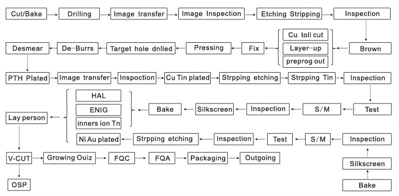
2.Multilayer Manufacture Process
…………… …………… ………………
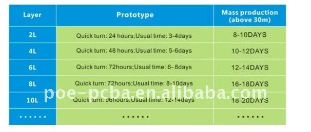
3.Leadtime for bare PCB
…………… …………… ………………
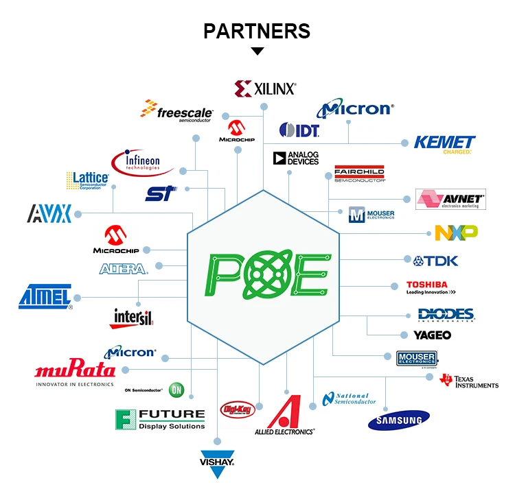
4.POE Partners
…………… …………… ………………
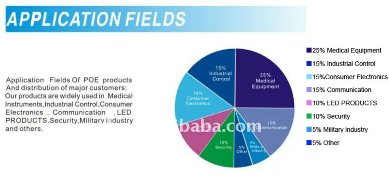
5. Application Fields&Customers
…………… …………… ………………
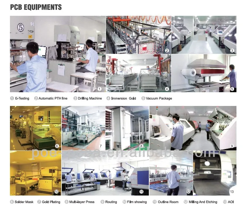
6.Production line
…………… …………… ………………
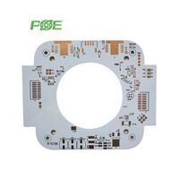
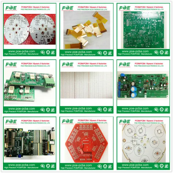
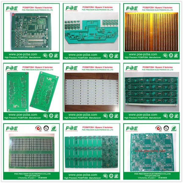
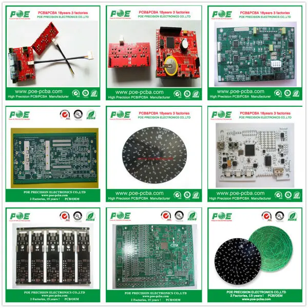
7.Products Show
…………… …………… ………………
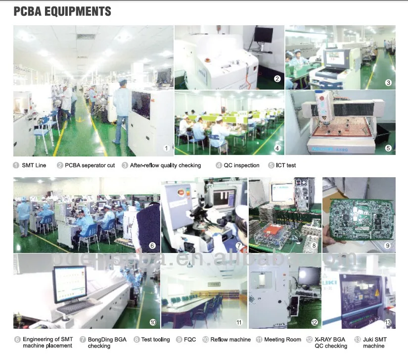
8.PCB&PCBA
…………… …………… ………………
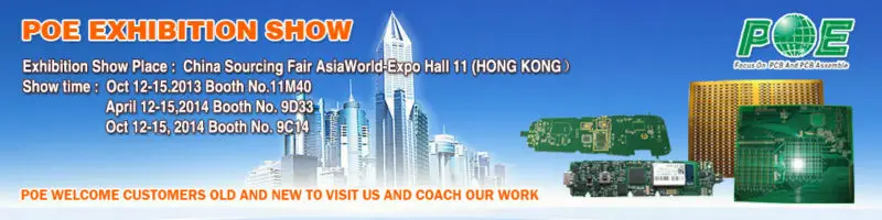
9. POE Invitation
10. PCB
-
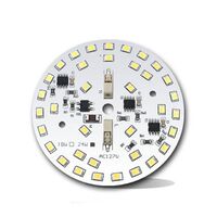
Customized single sided round aluminum substrate, 12v led light circuit board factory

-
Support professional double-sided PCB design one-stop OEM service
-
Custom electronics contract manufacturing double sided pcb assembly
-
Wholesale Lighting Led Pcb Led Board Design Led Circuit Board 3535 5730 3w 5w 7w 9w 12w 15w 18w Smd LED Printed Circuit Board
-
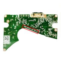
Free Shipping 100% Original HDD PCB Logic Board 2060-800041-003 REV P1 Hard Drive Circuit Board 2060-800041-000 REV P1
-
best china kb 3151c fr-1 pcb with rohs long life
-
China Printed Circuit Board Automotive Mobile Medical PCBA Assembly PCB Design Service
-
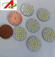
RDS Electronics- Circular board PCB aluminum factory MCPCB 2835 LED SMD 5630 aluminum PCB
-
5G mobile phone FR4 PCB manufacturer Shenzhen
-
Shenzhen ODM double-sided PCB designer and Customized PCB Manufacturer
Other Products
-
$0.50 - $3.00 / piece
-
$0.10 - $10.00 / piece
-
$1.00 - $15.00 / piece
-
$0.15 - $5.00 / piece
-
$0.50 / piece
-
$0.50 - $10.00 / piece
-
$0.10 / piece
-
$0.10 / piece
-
$0.25 / piece
-
$0.25 / piece