- Products
- Products
- Companies
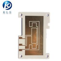
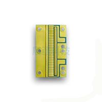
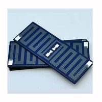
0.635 mm 96% AL2O3 ceramic PCB with printed resistors printed directly on board

-
Supplier: Shenzhen Danyu Electronics Co., Ltd. -
Region: Guangdong, China -
Contact: Mr Peter Gui -
Price: $1.99 / 100 - 499 pieces
$1.49 / >=500 pieces -
Min. Order: 100 pieces
Product details
| Copper thickness: | 10-20 microns | Substrate: | AlN/Si3N4/Al2O3(96%)/ZTA(ZrO29%) |
| Origin: | Guangdong, China | Packaging Details: | 10pcs/box, 10boxes/carton |
| Solder Mask: | No | product name: | AMB ceramic PCB |
| minute. Line spacing: | 0.15 mm | brand: | Danyu |
| model: | DSC00509 | Plate thickness: | 0.635mm |
| type: | Ceramic PCB | Silkscreen: | No |
| minute. Hole size: | 0.10 mm | Operating temperature: | -55℃~650℃ |
| Maximum Copper Thickness: | 800 microns | Board size: | Customization |
| Surface treatment: | ENEPIG | Material: | Silicon nitride |
| Certificate: | ISO13485/IATF16949/ISO9001/UL | Copper thickness: | 0.6 mm (600 microns) |
| Shipping method: | DHL UPS EMS TNT FedEx | minute. line width: | 0.15 mm |
| port: | Yantian | application: | New energy vehicle IGBT module |
| payment terms: | Western Union, T/T |
Product Description

The conductor thickness of this ceramic PCB is 5-7um gold paste

This is a ceramic PCB made with AMB (Active Metal Brazing) technology with very thick copper

This AMB ceramic PCB with plated through holes

This ceramic PCB substrate is 0.635mm 96% AL2O3

Compared with DBC technology, AMB technology has stronger thermal conductivity, heat resistance and impact resistance

The ceramic PCB is double-sided
This is a very good and suitable ceramic PCBmedical device
about Us

Major equipment

Customer visit

Manufacturing capacity

thing | Thick film capability | DCB/DBC capability | data transfer capability | Magnetic Bearing Capability | |||
layers | 10 floors | 2 layer | 2 layer | 2 layer | |||
board size | 200*200mm | 138*178mm | 138*190mm | 114*114mm | |||
Minimum plate thickness | 0.25 mm | 0.30mm~0.40mm | 0.25 mm | 0.25 mm | |||
Maximum plate thickness | 2.0 mm | 1L: 1.3mm; 2L: 1.6mm | 2.0 mm | 1.8 mm | |||
Conductor Thickness | 5 microns - 13 microns | 3.9 oz - 8.6 oz | 2 microns-200 microns | 8 oz - 22.9 oz | |||
Minimum Line Width/Space | 6/8 mil (0.15/0.20 mm) | 12/12 mil (0.30/0.30mm) | 6/8 mil (0.15/0.20 mm) | 20/20 mil (0.50/0.50 mm) | |||
Substrate type | AI203, ALN, BeO, ZrO2 | AI203, ALN, ZrO2 | AI203, ALN, ZrO2, Si3N4 | Aluminum Nitride, Silicon Nitride | |||
Substrate thickness | 0.25, 0.38, 0.50, 0.635, 0.80, | 0.25, 0.38, 0.50, 0.635, 0.76, | 0.25, 0.38, 0.50, 0.635, 0.80, | 0.25, 0.38, 0.50, 0.635, 0.76, | |||
1.0, 1.25, 1.5, 2.0mm | 1.0 mm | 1.0, 1.25, 1.5, 2.0mm | 1.0mm | ||||
minimum aperture | 4 million (0.1mm) | ||||||
Minimum pitch | NPTH: 16mil (0.30mm); PTH: 20mil (0.5mm) | ||||||
Minimal pad ring (single) | 6 million (0.15mm) | not applicable | 3 million (0.075mm) | not applicable | |||
Plated Through Hole Wall Thickness | 4 million (10 microns) | not applicable | 4 million (10 microns) | not applicable | |||
Minimum Pad Diameter | 10 million (0.25mm) | 8 million (0.20mm) | 6 million (0.15mm) | 8 million (0.20mm) | |||
Minimum Solder Bridge | 12 million (0.30mm) | 8 million (0.20mm) | 6 million (0.15mm) | 8 million (0.20mm) | |||
Minimum BAG PAD margin | 12 million (0.30mm) | 8 million (0.20mm) | 5 million (0.125mm) | 8 million (0.20mm) | |||
PTH/NPTH diameter tolerance | Plated Through Hole: ±4 mil (0.1 mm); NPTH: ±2 mil (0.05 mm) | ||||||
Hole position deviation | ± 4 mil (0.1 mm) | ||||||
Shape Tolerance | Laser: +0.2/0.05mm; | Laser: +0.2/0.05mm | Laser: +0.2/0.05mm; | Laser: +0.2/0.05mm | |||
Die: +0.25/0.20mm | Die: +0.25/0.20mm | ||||||
Line Width/Space Tolerance | ± 5 mil (0.125 mm) | ± 5 mil (0.125 mm) | ± 1 mil (0.025 mm) | ± 5 mil (0.125 mm) | |||
surface treatment | Silver palladium, gold palladium, manganese/nickel | OSP/nickel plating, ENIG | OSP/ENIG/ENEPIG | OSP/nickel plating, ENIG | |||
Thermal Stress | 1 hour @350℃ | 3 x 10 sec @ 280°C | 15 minutes @350℃ | 3 x 10 seconds @ 280°C | |||
Advantage

Packaging and Shipping

Customer Reviews

VIEW MORE
You may like
-
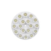
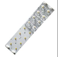
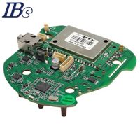
Fuel meter resistor chip fuel power resistor board resistor chip circuit board customization - manufactured fuel meter thick film circuit

-
Ceramic PCB Shenzhen black yellow green gold red white blue copper button mask silk screen electronic layer surface solder ROHS
-
DBC ceramic substrate DPC film double-sided circuit board
-
High Quality Custom Product Bom Gerber Quote Multilayer Aluminum Nitride Substrate PCB Supplier Ceramic PCB Manufacturer
-
2L DBC Ceramic PCB Circuit Thick Film Multilayer Aluminum Ceramic Substrates Heavy Duty Copper Strip
-
Black porcelain aluminum nitride ceramic substrate High thermal conductivity Strong bonding force High insulation
-
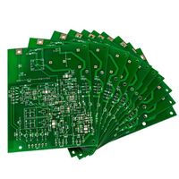
Custom ceramic PCB supplier from electronic component factory offers PCB prototype
-
Factory selling all kinds of custom lap board Pcb circuit board Pcb supplier
-
Non-toxic and harmless environmental protection aquarium coral debris plug ceramic base
-
High frequency ceramic pcb antenna prepreg pcb
Other Products
-
$0.40 - $0.60 / piece
-
$0.30 - $0.50 / piece