- Products
- Products
- Companies
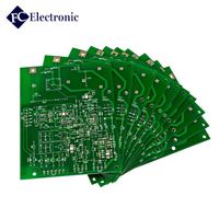
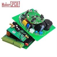
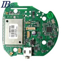
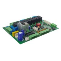
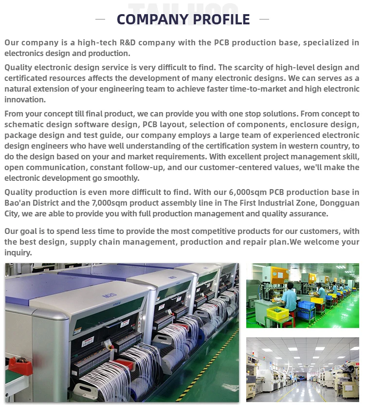
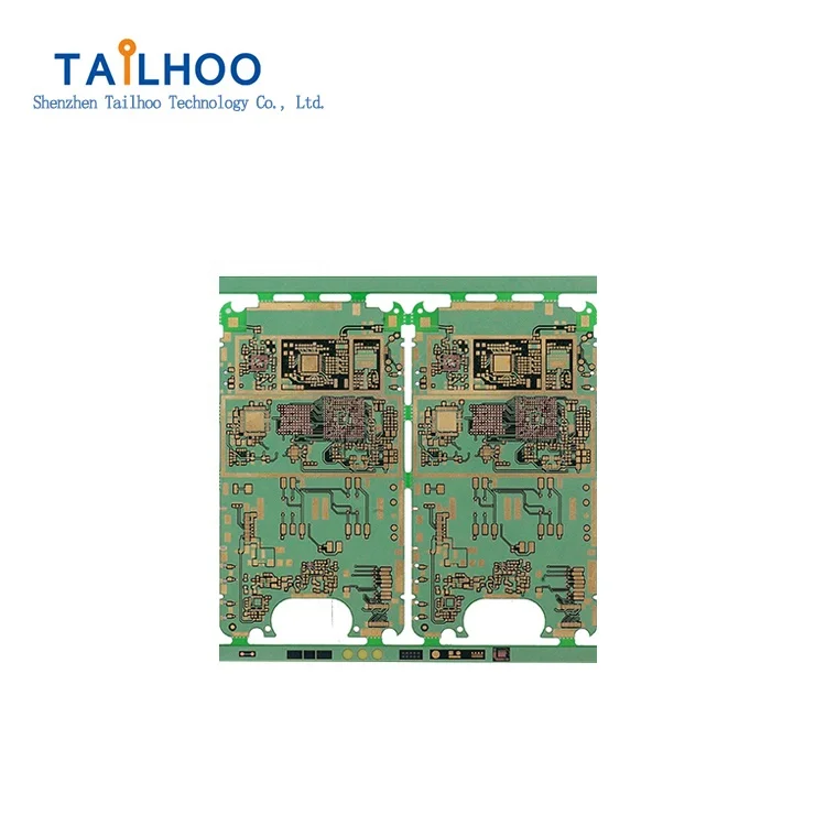
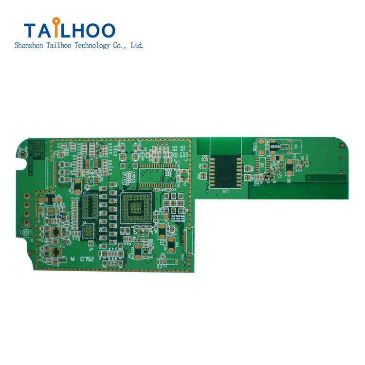
Shenzhen Double-sided PCB Manufacturer

-
Supplier: Shenzhen Tailhoo Technology Co., Ltd. -
Region: Guangdong, China -
Contact: Mr Ted Zeng -
Price: $0.10 / >=2 pieces -
Min. Order: 2 pieces
Product details
| Min. Line Width: | 0.1mm; | Packaging Detail: | Buble Bag/Vacuum Package/Pearl wool and Carton; |
| Surface Finishing: | HASL; | Place of Origin: | Guangdong China; |
| Solder Mask: | Green; | Certificate: | ROHS. CE; |
| Model Number: | TH-PCB-723; | Board Size: | 800mmx600mm; |
| Supply Ability: | 30000 Square Meter/Square Meters per Month; | PCBA Test: | X-ray,AOI Test,Functional test; |
| Board Thickness: | 1.6mm; | Port: | Shenzhen; |
| Product Name: | Double-sided PCB; | Base Material: | FR-4; |
| Copper Thickness: | 1oz; | Type: | Double-sided PCB; |
| Number of Layers: | 2 Layer; | Brand Name: | TH; |
| Min. Hole Size: | 0.2mm; | Min. Line Spacing: | 0.1mm; |
| PCB Test: | Test-rig,Flying Probe Test; | Silkscreen: | White; |
| Payment Terms: | L/C,Western Union,T/T,MoneyGram,Paypal; |
Shenzhen Double-sided PCB Manufacturer


| Item | Specification | |
| 1 | Numbr of Layer | 1-18Layers |
| 2 | Material | FR-4,FR2.Taconic,Rogers, CEM-1 CEM-3,ceramic , crockery Metal-backed Laminate |
| 3 | Surface Finish | HASL(LF), Gold plating, Electroless nickel immersion gold, Immersion Tin, OSP(Entek) |
| 4 | Finish Board Thickness | 0.2mm-6.00 mm(8mil-126mil) |
| 5 | Copper Thickness | 1/2 oz min;12 oz max |
| 6 | Solder Mask | Green/Black/White/Red/Blue/Yellow |
| 7 | Min.Trace Width & Line Spacing | 0.075mm/0.1mm(3mil/4mil) |
| 8 | Min.Hole Diameter for CNC Driling | 0.1mm(4mil) |
| 9 | Min.Hole Diameter for punching | 0.9mm(35mil) |
| 10 | Biggest panel size | 610mm*508mm |
| 11 | Hole Positon | +/-0.075mm(3mil) CNC Driling |
| 12 | Conductor Width(W) |
0.05mm(2mil)or; +/-20% of original artwork |
| 13 | Hole Diameter(H) |
PTH L:+/-0.075mm(3mil); Non-PTH L:+/-0.05mm(2mil) |
| 14 | Outline Tolerance |
0.125mm(5mil) CNC Routing; +/-0.15mm(6mil) by Punching |
| 15 | Warp & Twist | 0.70% |
| 16 | Insulation Resistance | 10Kohm-20Mohm |
| 17 | Conductivity | <50ohm |
| 18 | Test Voltage | 10-300V |
| 19 | Panel Size | 110×100mm(min);660×600mm(max) |
| 20 | Layer-layer misregistration |
4 layers:0.15mm(6mil)max; 6 layers:0.25mm(10mil)max |
| 21 | Min.spacing between hole edge to circuity pqttern of an inner layer | 0.25mm(10mil) |
| 22 | Min.spacing between board oulineto circuitry pattern of an inner layer | 0.25mm(10mil) |
| 23 | Board thickness tolerance |
4 layers:+/-0.13mm(5mil); 6 layers:+/-0.15mm(6mil) |
| 24 | Impedance Control | +/-10% |
| 25 | Different Impendance | +-/10% |

Q1.What do we need for PCB or PCBA quotation?
PCB: Gerber files/PCB files, Quantity, Board processing details( board material, thickness, copper thickness, surface treatment, color of solder mask and silkscreen)
PCBA: Above PCB info, BOM with components specs, testing doc if you have
Q2. Do we have MOQ?
There is no MOQ in TAILHOO. We are able to produce Small volume as well as large volume production with flexibility.
Q3. Are my files safe?
Yes. All of our client’s design files are classified and safe. And we’ll not share with third party. If NDA needed, we’ll sign.
Q4. If the product fails after receive, what should I do?
We will be responsible for all of the product we send out. If you have sent us test docs, we’ll gurantee 0% defective rate, which means if you receive defective ones, we will be responsible for it. If you don’t have test docs, we’ll gurantee 0.3% defective rate.
Q5, If I only have samples, can I produce it?
Yes. We can copy it and produce based on your samples.
Q6.Shipping cost?
The shipping cost is depend on the destination, weight, packing dimension. We can quote you when production finish, or even before production starting.
VIEW MORE
You may like
-
Manufacturing custom design multi -layer HDI PCB and PCBA assembly plants for medical equipment for medical equipment
-
One Stop PCB Service Printed Circuit Factory Custom Multilayer PCBA Board All PCB Assembly and Manufacturing
-
Multilayer PCB Assembly Manufacturer ShenZhen Electronics SMT PCBA Factory
-
Shenzhen Customize PCB PCB Circuit Multilayer Pcb Manufacturer
-
Manufacturer PCB Circuit Board Assembly Professional Customer Printing Prototyping Factory Multilayer PCB and PCBA
-
Electronics Factory Multilayer Printed Circuit Board Manufacturer OEM ODM PCBA PCB Manufacturer Offer Electronic PCB Design
-
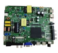
Original brand new TP.MS358.PB801 4-core wifi network 32--50 inch universal three-in-one motherboard suitable for smart TV accessories
-
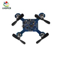
Support one stop service Oem Professional Pcba Drone Pcb Drone Pcba
-
Cem-1 94v0 pcb schematic circuit board design services
-
Wind source dual system swimming pool heat pump constant temperature controller CC395 CCYCKB001