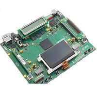
- Products
- Products
- Companies
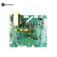
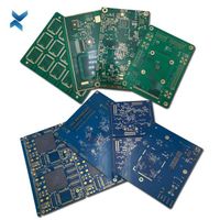
Electronic led light PCB board

-
Supplier: Shenzhen Fulltronics Technology Co., Ltd. -
Region: Guangdong, China -
Contact: Mr Jasen Ho -
Price: $0.10 / >=5 pieces -
Min. Order: 5 pieces
| Number of Layers: | Single, Double, Multilayers; | Min. Hole Size: | 0.1mm; |
| Board Thickness: | 0.5~3.2mm; | Min. Line Width: | 0.1mm; |
| Port: | Shenzhen, HongKong; | Supply Ability: | 50000 Square Meter/Square Meters per Month Electronic led buld pcb , led light bulds 94v0 pcb board design; |
| Brand Name: | Fulltronics; | Product name: | led bulb pcb; |
| Payment Terms: | L/C,Western Union,D/P,D/A,T/T,MoneyGram,Paypal; | Silkscreen: | White; |
| Name: | Electronic led buld pcb , led light bulds 94v0 pcb board design; | Copper Thickness: | 1oz~4oz; |
| packing: | Vacuum+Dessicant for inner pack; | PCB Item: | Fr4 94V0 Rohs Pcba Pcb; |
| Place of Origin: | Guangdong China; | Board Size: | customized; |
| Packaging Detail: | Vaccum package and standard carton outside Electronic led buld pcb , led light bulds 94v0 pcb board design; | Model Number: | FC-pcb044; |
| Certificate: | RoHS, U L, S GS, ISO/TS16949, ISO9001; | Surface Finishing: | HASL; |
| Min. Line Spacing: | 0.1mm; | Base Material: | FR-4 94v0,FR-4; |
| Type: | rigid pcb; | Soldermask: | Green, White, Red, Brown, Black; |
| Lead Free Technology: | Yes; |

Our production capacity
| PCB Item | Manufacture Capacity |
| Layer Counts | 1--20L |
| Base Material | FR4,High-TG FR4,CEM3,aluminum,High Frequency(Rogers,Taconic,Aron,PTFE,F4B) |
| Material Thickness(mm) | 0.40, 0.60, 0.80, 1.00, 1.20, 1.50, 1.60, 2.0, 2.4, 3.2 |
| Max board size(mm) | 1200x400mm |
| Board Outline Tolerance | ±0.15mm |
| Board Thickness | 0.4mm--3.2mm |
| Thickness Tolerance | ±8% |
| Minimum line/space | 0.1mm |
| Min Annular Ring | 0.1mm |
| SMD Pitch | 0.3mm |
| Holes | |
| Min Hole Size(mechanical) | 0.2mm |
| Min Hole Size(laser hole) | 0.1mm |
| Hole Size Tol (+/-) | PTH:±0.075mm;NPTH: ±0.05mm |
| Hole Position Tol | ±0.075mm |
| Plating | |
| HASL/LF HAL | 2.5um |
| Immersion Gold | Nickel 3-7um Au:1-5u'' |
| Surface Finish | HAL,ENIG,Plated Gold,Immersion Gold,OSP |
| Copper | |
| Copper Weight | 0.5--6oz |
| Color | |
| Solder mask | Green, Blue, Black, White, Yellow, Red, Matt Green, Matt Black, Matt Blue |
| Silk screen | White, Black, Blue,Yellow |
| Acceptable File Format | Gerber file,Powerpcb,CAD,AUTOCAD,ORCAD,P-CAD,CAM-350,CAM2000 |
| Certificate | ROSH,ISO9001,UL |
LEAD TIME FOR PRODUCTION ORDERS:
|
Sample Lead time |
Mass production lead time |
|
|
Single sided PCB |
1~3 |
4~7 |
|
Double sided PCB |
2~5 |
7~10 |
|
Multilayer PCB |
7~8 |
10~15 |
|
PCB and Assembly |
8~15 |
15~20 |
OEM/ODM/EMS Services for PCBA:
- PCBA, PCB Board assembly: SMT & PTH & BGA
- PCBA and enclosure design
- Components sourcing and purchasing
- Quick prototyping
- Plastic injection molding
- Metal sheet stamping
- Final assembly
- Test: AOI, In-Circuit Test (ICT), Functional Test (FCT)
- Custom clearance for material importing and product exporting
Capability - SMT
- Lines 9(5 Yamaha,4KME)
- Capacity 52 million placements per month
- Max Board Size 457*356mm.(18”X14”)
- Min Component size 0201-54 sq.mm.(0.084 sq.inch),long connector,CSP,BGA,QFP
- Speed 0.15 sec/chip,0.7 sec/QFP
Capability - PTH
- Lines 2
- Max board width 400 mm
- Type Dual wave
- Pbs status Lead-free line support
- Max temp 399 degree C
- Spray flux add-on
- Pre-heat 3
Product Type


To ensure an accurate quote, be sure to include the following information for your project:
•Complete GERBER files including the BOM list
•Other file types (Altium,Protel,OrCAD)
•"Read Me" notes for additional fabrication information
•Quantities
•Turn time
•Panelization Requirements
•Materials Requirements
•Finish requirements
Your custom quote will be delivered in just 2-24 hours, depending on the design complexity.

AOI Testing
Checks for solder paste
Checks for components down to 0201"
Checks for missing components, offset, incorrect parts, polarity
X-Ray Inspection
X-Ray provides high-resolution inspection of:
BGAs
Micro BGAs
Chip scale packages
Bare boards
In-Circuit Testing
In-Circuit Testing is commonly used in conjunction with AOI minimizing functional
defects caused by component problems.
Power-up Test
Advanced Function Test
Flash Device Programming
Functional testing

We purchase material from Original Company and distributers.
We make products by strict engineer processes.
We have strict inspection processes.
We send products by vaccum package,antistatic package and carton box.


1. Are my design files secure when I send them to you?
Your files are held in complete safety and security.Your files are never shared nor will any third parties have access to your design files.Fulltronics can sign an NDA(Non-disclosure agreement) before sending files.
2. For small quantity orders, can you produce prototype PCBs?
Yes. Fulltronics can produce prototypes. but the greater the quantity, the greater the cost savings.
3. What file formats do you accept for PCB and assembly?
Gerber ,CAM Auto CAD DXF, DWG formats.
4. Do you have after-sales product servicing available for your customers?
Yes, for any quality problems Fulltronics will take our responsibility to solve it for you any time.
-
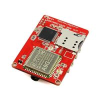
Anti-Theft TV Laptop Mini GPS Tracking Device GT01 Mini GSM GPS Tracker PCBA Board for Bicycle/Motorcycle/Scooter/Vehicle

-
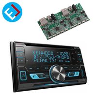
El Car Radio Smt/Dip Car Equipment Multilayer PCB Control Board Prototype Car Radio Pcba Assembly
-
PCB Manufacturer 94v0 Scrap PCBA Manufacturer PCB Board
-
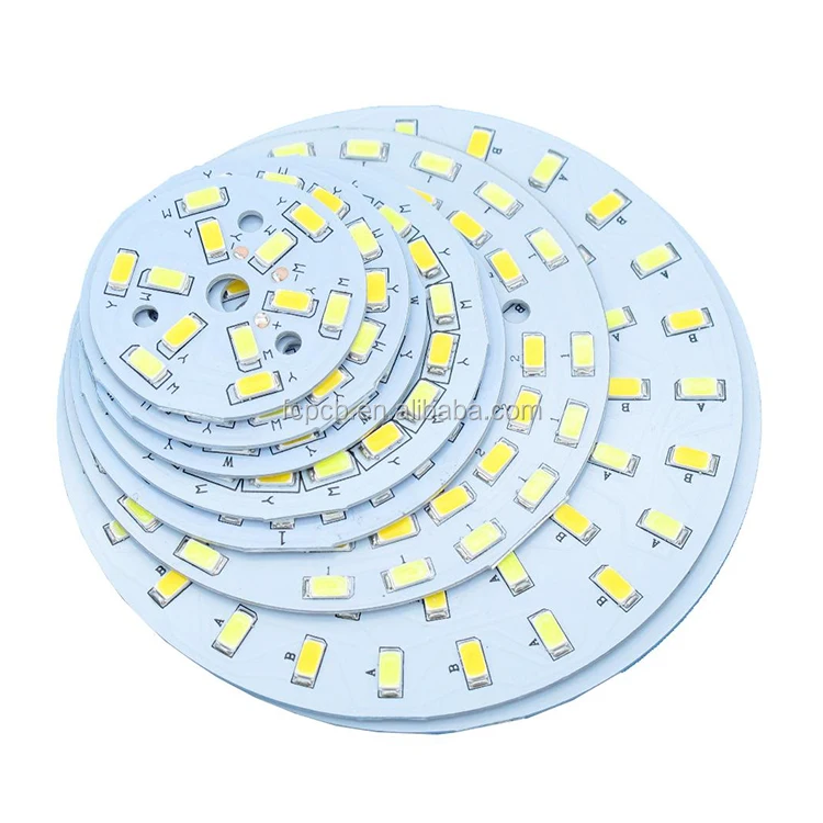
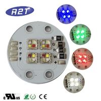
CREE XML Full Color RGBW SMD5050 LED Light PCB Board Assembly
-
Mega2560 ATMEGA16U2 / Pro Mini MEGA 2560 Mega+WiFi R3 ATmega2560 CH340G Chip For Arduino UNO R3 WeMos ESP8266 Development Board
-
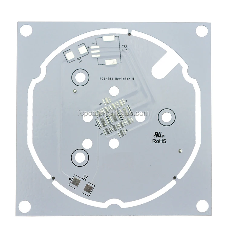
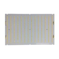
High Efficiency LM281B+ VK Pro LED PCB Board
-
Pulse Induction Metal Detector PI Metal Detector PCBA Assembly
-
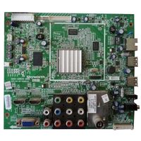
Professional pcb manufacturing for samsung tv spare parts
-
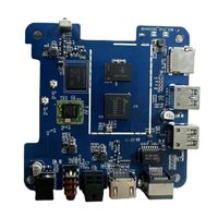
4GB Ram 32GB 64GB Rom 4k Internet Pcba S905X BGA388 AMLOGIC 905X S905 CPU S905 BGA Quad Core 64-bit Chip New Original Sold
-
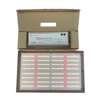
Custom LED board for LED grow light

Other Products
-
$0.10 - $10.00 / piece
-
$0.10 / piece
-
$0.10 / piece
-
$0.10 / piece
-
$0.99 / piece