- Products
- Products
- Companies
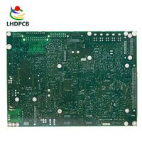
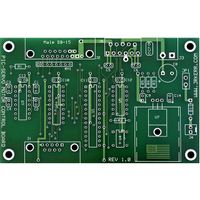
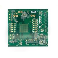
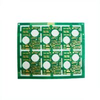
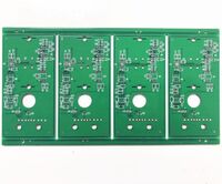
PCB placa/ High Quality Electronic Card / Printed Circuit Board / PCBA

-
Supplier: Shenzhen DYC Electronic Technology Co., Ltd. -
Region: Guangdong, China -
Contact: Mr Spancer Huang -
Price: $1.00 / >=5 pieces -
Min. Order: 5 pieces
Product details
| Place of Origin: | Guangdong China ; | Surface Finishing: | HASL ; |
| Min. Line Width: | 0.12mm ; | Min. Hole Size: | 0.004" ; |
| Supply Ability: | 60000 Square Meter/Square Meters per Month ; | Packaging Detail: | Packaging Details: Inner packing: Vacuum and Anti-static bubble bag. Outer packing: High standard cartons box. Delivery Details: Sample5-7 days; Mass:15-25days ; |
| PCB Item: | High Quality Electronic Card/PCB placa ; | Payment Terms: | T/T,Western Union ; |
| Base Material: | FR4 ; | Port: | shenzhen/Hongkong ; |
| Certificate: | ROSH. ISO9001 ; | Model Number: | pcba ; |
| Min. Line Spacing: | 0.01mm ; | Board Thickness: | 1.6mm ; |
| Surface finishing: | HASL ; | Copper Thickness: | 0.25 Oz -12 Oz ; |
| Type: | Multilayer Printed Circuit Board ; | Solder mask color: | Green ; |
| Brand Name: | DYC ; | Item: | Pcb Electronic Contract Manufacturing Printing Circuit Boards ; |
PCB placa/ High Quality Electronic Card / Printed Circuit Board / PCBA
About DYC
DYC 2007-2018, 11 YEARS PCB PCBA ONE STOP SERVICE

| Established time | Aug 2007 |
| Number of emplooyes | 250 |
| Factory area | 15,000 sqm |
Location: 6,7 floor, Yuxing Second7 floor, Yuxing Second industrial park, xixiang, Bao'an district, Shenzhen. | Near by shenzhen airport, 15 minutes. |
| Near by Hongkong airport, 74 km. | |
| Near by shekou terminal, 22 km. | |
| Fabrication | 8 million spot SMT/day. |
| Certification | ISO9001-2008, CE, RoHS. |
| Sales avenue | 0.3 billion |
6 SMT Lines, 2 DIP lines, 2 end-products assembly lines

DYC services


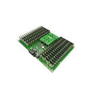
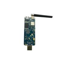
PCBA manufacture
PCBA CAPACITY
| Max size of pcb board | 500* 400mm |
| Max thickness | 3mm |
| Min thickness | 0.5mm |
| Min chip | 1005 |
| Max SMD components weight | 100g |
| Max part height | 25 mm |
| Max part size | 150*150 mm |
| Min pin space | 0.3mm |
| Max BGA components space | 0.3mm |
| Max BGA components space | 0.3mm |
| Max SMD accuracy | 25um@ IPC |
| SMD capacity | 8 Million point/day |
How to make your PCBA

PCBA flow:

Strength of PCBA manufacture

FAQ:
Q: What should i provide to get one PCB quotation?
A: Gerber file, PCB technical, quantity and bom list.
Q: Will you check my files before production?
A: Yes, our engineer will check your gerber file and BOM list to avoid any mistake.
Q: What's the lead time for PCBA?
A: 8-10 days for sample, 15-20 days for bulk order.
Q: My budget is limited, can you provide solutions to save cost ?
A: Yes, we can. For example: Replace the DIP components with SMD components, so it can narrow the PCB board size to save cost. Relayout the pcb to reduce the size, it can save cost, Also we can recommend you alternative components.
Q: Do you have any other special discount ?
A: Yes, we provide free panel, free test and free packaging.
Testing equipment

More information
Customer feedback:

You may also like:
 |  |  |
If you have more questions, please clic to contact us

VIEW MORE
You may like
-
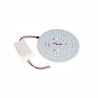
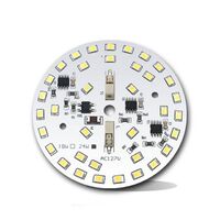
Customized single sided round aluminum substrate, 12v led light circuit board factory

-
Support professional double-sided PCB design one-stop OEM service
-
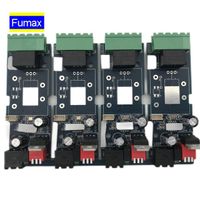
Custom electronics contract manufacturing double sided pcb assembly
-
Wholesale Lighting Led Pcb Led Board Design Led Circuit Board 3535 5730 3w 5w 7w 9w 12w 15w 18w Smd LED Printed Circuit Board
-
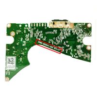
Free Shipping 100% Original HDD PCB Logic Board 2060-800041-003 REV P1 Hard Drive Circuit Board 2060-800041-000 REV P1
-
best china kb 3151c fr-1 pcb with rohs long life
-
China Printed Circuit Board Automotive Mobile Medical PCBA Assembly PCB Design Service
-
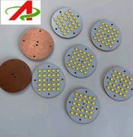
RDS Electronics- Circular board PCB aluminum factory MCPCB 2835 LED SMD 5630 aluminum PCB
-
5G mobile phone FR4 PCB manufacturer Shenzhen
-
Shenzhen ODM double-sided PCB designer and Customized PCB Manufacturer
Other Products
-
$20.00 / piece
-
$0.80 / piece
Related Search
high quality semi auto printing slotting machine
2 layer immersion gold printed circuit board suppliers
multi layer print circuit board suppliers
fr4 printed circuit board suppliers
printed circuit boards
flexible printed circuit boards manufacturers
inform print circuit board suppliers
high quality pcb electronics
high quality fpc flexible circuit
high quality circuit design