- Products
- Products
- Companies
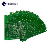
Professional double side pcb maker,electronic pcb design,copy and assembly

-
Supplier: Cireemax (shenzhen) Technology Ltd. -
Region: Guangdong, China -
Contact: Mr Tony Cheng -
Price: $1.00 /piece -
Min. Order: 1 piece
| Number of Layers: | 4-Layer; | Surface Finishing: | HASL, ENIG, Immersion Gold, etc.; |
| Certificate: | UL/ROHS/ISO9001; | Copper Thickness: | 1oz; |
| Brand Name: | Circuit Boards Supplier; | Board Thickness: | 1.6mm-3.2mm; |
| Delivery Detail: | 7days for Printed Circuit Boards samples; | Surface Finish: | HASL; |
| Application: | 94v0 Led Pcb; | Material: | FR4/CEM-1/CEM-3/FR1/aluminum; |
| Base Material: | FR-4/aluminum/ceramic/cem-3/FR-1; | Min. Line Width: | 0.1mm(Flash Gold)/0.15mm(HASL); |
| Min. Hole Size: | 0.20mm; | Product name: | double side pcb; |
| Thickness: | 1.6mm; | Port: | Shenzhen/Hongkong; |
| Layer: | 1-24layers; | Copper Thickness: | 0.3oz-3oz; |
| Supply Ability: | 10000 Piece/Pieces per Week Electronic PCB Assembly; | Place of Origin: | Guangdong China; |
| Min. Line Spacing: | 0.1um(3mil); | Payment Terms: | L/C,D/A,D/P,T/T,Western Union,MoneyGram,Paypal; |
| Type: | Circuit Boards Supplier; | Model Number: | Printed Circuit Boards; |
| Solder Mask: | Green. Red. Blue. White. Black.Yellow; | Packaging Detail: | Inner packing: Vacuum packing / Plastic bag for electronic 94v0 pcb Outer packing: Standard carton packing; |
Professional double side pcb maker,electronic pcb design,copy and assembly
Why Choose Us
•QUICK RESPONSE & DELIVERY
•CHEAPER WHILE GOOD QUALITY
•SMALL QUANTITY RUNS
•CERTIFIED MANUFACTURING CAPACITY
•GLOBAL IC & COMPONENT SOURCING
•ONE-STOP PCB & PCBA SERVICE
Ciree (Subordinated to SATECH) is a professional manufacturer of PCB & PCBA and EMS (electronics manufacturing service) with nearly 15-year experience in PCB Design & Layout, PCB Fabrication, PCB Assembly, PCBA Prototype, PCBA Test, Electronic Part Sourcing and EMS for kinds of smart electronic manufacturing.
SMT Processing
Now we have 8 SMT Lines and 3 DIP Lines to perform PCB assembly. The precision of chip replacement is up to +0.1MM, this indicates we have professional skills in producing all kinds of printed integrated circuit boards such as SO, SOP, SOJ, TSOP, TSSOP, QFP, BGA and U-BGA with surface-mount technology (SMT), thru-hole technology (THT) and merged tech components.
DIP Processing
Ciree has three DIP processing lines, professional working platforms and carriers, this ensures a output capacity of 1 500 000pcs per day. For every process, technical and standard operation guidelines are made to follow, with strict KPI, this makes sure of 99.8% of pass for every PCBA. Lower our rejects, create more value for clients.


What We Are Doing


PCB Design & Layout
» Excellent Expertise in design tools: Allegro, Pads, and Mentor Expedition.» High density SMT designs (BGA, uBGA, PCI, PCIE, CPCI…)
» Flex PCB designs of all sorts
» Complete assembly drawings
» In-Circuit Test data generation (ICT)
» Drill, panel and cutout drawings designed
» Professional fabrication documents created
» High-speed, multi-layer digital PCB designs- Bus routing, differential pairs, matched lengths; Fast PCB design in 2-3 days.
» Concentrate on the PCB design Wi-Fi Module, BLE Module, GPS Tracking application.RF Modules,Medical-Care devices,LED PCB Boards.
» We come up with the design as per customer requirement,and take care for the RAW material cost at the outset of design.
» Full control for the PCB design, from requirement, Schematic, PCB Layout, SI/PI/EMI inspection, we will locate the design issues in the inspection processing.


| PCB layer | 1, 2, 4 or 6, up to 18 layers | |||||||
| Board shape | Rectangular, round, slots, cutouts, complex, irregular | |||||||
| Board type | Rigid, flexible, rigid-flexible | |||||||
| Board material | FR-4 glass epoxy, FR4 High Tg, RoHS compliant; Aluminum, Rogers, etc. | |||||||
| Board cutting | Shear, V-score, tab-routed | |||||||
| Board thickness | 0.2 ~ 4.0 mm (±10%), Flex board: 0.01 ~ 0.25″ (±10%) | |||||||
| Copper weight | 1.0, 1.5, 2.0 Oz (tolerance ±0.25 oz) | |||||||
| Solder mask | Double-sided green LPI, Also support red, white, yellow, blue, black | |||||||
| Silk screen | Double-sided or single-sided in white,yellow, black, or negative | |||||||
| Silk screen min. line width | 0.006″ or 0.15mm | |||||||
| Max board dimension | 20 inch *20 inch or 500mm*500mm | |||||||
| Min. trace/gap | 0.10mm, or 4 mils | |||||||
| Min. drill hole diameter | 0.01”, 0.25mm, or 10 mils | |||||||
| Surface finish | HASL, Nickle, Imm Gold, Imm Tin, Imm Silver, OSP etc. | |||||||
| Min.slot width | 0.12”, 3.0 mm, or 120 mils | |||||||
| V-score depth | 20-25% of board thickness | |||||||
| Plated through holes | Yes | |||||||
| Design file format | Gerber RS274X, 274D, Eagle and AutoCAD’s, DXF, DWG, Protel 99se | |||||||
| Order Types/PCB Layers | 1/2-layer | 4-layer | 6-layer | Above 8-layer | HDI | ||||||
| Normal Sample Orders | 5-6 days | 6-7 days | 7-8 days | 10-12 days | 15-20 days | ||||||
| Fast Sample Orders | 48-72 hours | 5 days | 6 days | 6-7 days | 12 days | ||||||
| First Batch Orders | 7-9 days | 10-12 days | 13-15 days | 16 days | 20 days |

Different types of Assembly
°THD (Thru-Hole Device)
°SMT (Surface-Mount Technology)
°SMT & THD combined
°2-sided SMT and THD assembly
Order Volume Allowed
°1 to 5,000 boards
Parts
°Passives parts, smallest size 0201
°Fine pitch to 8 Mils
°BGA, uBGA, QFN, POP and Zero-Lead chips
°Connectors and terminals
Component Package
°Reels
°Cut tape
°Tube and tray
°Loose parts and bulk
PCB Board Measurements
°Minimum measurement: 0.2″ x 0.2″ (5mm x 5mm)
°Largest dimension: 15″ x 20″ (381mm x 508mm)
Printed circuit board shapes
°Oblong
°Round
°Slots and Cut outs
°Complicated and Uncommon
PCB board kinds
°Rigid FR-4 boards
°Rigid-Flex boards
Assy procedures
°Leaded process
°Zero-Lead (RoHS)
Design file formatting
°Gerber RS-274X, 274D, Eagle as well as AutoCAD’s DXF, DWG
°BOM (Bill of Materials) (.xls, .csv, . xlsx)
°Centroid (Pick-N-Place Or XY file)
Testing Processes
°Visual Inspection
°X-ray Inspection
°AOI (Also known as: Automated Optical Inspection)
°ICT (AKA: In-Circuit Test)
°Functional testing
Turnaround time periods
°1 To 5 days for only printed circuit board assy
°10 To16 days for full Turnkey Circuit Card Assy
•Rapid Turnaround •Prototype/Production Support •Blank Boards»Components»Assembly •Rapid On-line Quote
Our PCBA test is a complete system which includes FCT, ICT, AOI and so on, so that we make sure each product out of our factory are consistent with the designed parameters and specifications. Before the PCB assembly, we always need to communicate with customers for the confirmation of a test plan. Usually our testing team will help our customers copy if they are pleased to hand over IC program, and then make FCT by testing jig which is usually customized according to PCB functions. (For full idea about FCT, ICT and AOI, you may know about them by Google.)
| Order Type | Testing Type | |||||
| PCB samples | Flying test and E-test | |||||
| PCB batch orders | Test complete production line by Testing jig and E-test | |||||
| PCBA samples | E-test, FCT or other test method provided by customers | |||||
| PCBA batch orders | Testing jig or testing program made for a whole production line, or other method from customers. | |||||
Component Sourcing Center
•Global IC Sourcing •Strong & Stable Component Supply Channels •Fast Component Purchasing •Scientific Inventory Management System
PCBA Cases


-
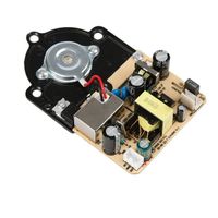
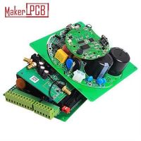
Manufacturing custom design multi -layer HDI PCB and PCBA assembly plants for medical equipment for medical equipment

-
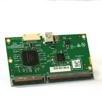
One Stop PCB Service Printed Circuit Factory Custom Multilayer PCBA Board All PCB Assembly and Manufacturing
-
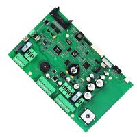
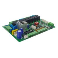
Multilayer PCB Assembly Manufacturer ShenZhen Electronics SMT PCBA Factory
-
Shenzhen Customize PCB PCB Circuit Multilayer Pcb Manufacturer
-
Manufacturer PCB Circuit Board Assembly Professional Customer Printing Prototyping Factory Multilayer PCB and PCBA
-
Electronics Factory Multilayer Printed Circuit Board Manufacturer OEM ODM PCBA PCB Manufacturer Offer Electronic PCB Design
-
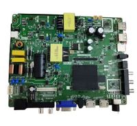
Original brand new TP.MS358.PB801 4-core wifi network 32--50 inch universal three-in-one motherboard suitable for smart TV accessories
-
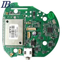
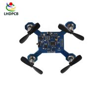
Support one stop service Oem Professional Pcba Drone Pcb Drone Pcba
-
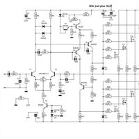
Cem-1 94v0 pcb schematic circuit board design services
-
Wind source dual system swimming pool heat pump constant temperature controller CC395 CCYCKB001