- Products
- Products
- Companies
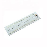
Aluminium Custom Cree SMD 3030 3535 LED PCB

-
Supplier: Shenzhen Feidaming Electronics Technology Co., Ltd. -
Region: Guangdong, China -
Contact: Ms. Linda Yu -
Price: $2.00 / >=1000 pieces -
Min. Order: 1000 pieces
| Packaging Detail: | polybag+carton for Aluminium Custom Cree SMD 3030 3535 LED PCB; | Place of Origin: | Guangdong China; |
| Min. Hole Size: | 0.25mm; | Surface Finishing: | HAL; |
| Min. Line Width: | 0.10(4mil); | MOQ: | 1000PCS; |
| Certificate: | CE,ROHS; | Min. Line Spacing: | 0.1mm4mil); |
| Payment Terms: | L/C,T/T,Western Union,paypal; | Model Number: | cree led pcb; |
| Copper Thickness: | 1 Oz; | LED Type: | SMD; |
| Thickness: | 1mm 1.5mm 2mm 3mm; | Board material: | 5052 Aluminum; |
| Product name: | Aluminium Custom Cree SMD 3030 3535 LED PCB; | Brand Name: | MOKO; |
| Solder mask: | WHITE; | Length: | OEM; |
| Board Thickness: | 1mm; | Layout: | Single; |
| Size: | OEM circuit board design; | Base Material: | Alu; |
| Port: | Shenzhen/hongkong; | Supply Ability: | 300000 Piece/Pieces per Week 24 hours is avainable; |

Aluminium Custom Cree SMD 3030 3535 LED PCB
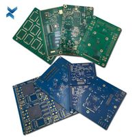
PCBA / LED PCBA / PCB Assembly / EMS service Manufacturer :
MOKO services:
- Contract Manufacturing
- Engineering Services
- PCB Fabrication
- Component sourcing
- PCB assembly
- Function test (for free)
- Plastics and Molds
MOKO advantages:
- ISO9001: 2008 certificates
- UL and ROHS certificates
- PCBA free function test
- PCBA with 2 years warranty
- 10 years producing experience
- 8 SMT lines and 4 Thru-hole lines
- 400 workers
Orientronic PCB assembly Equipment:
- SMT Machine: SIEMENS SIPLACE D1/D2 / SIEMENS SIPLACE S20/F4
- Reflow Oven: FolunGwin FL-RX860
- Wave Soldering Machine: FolunGwin ADS300
- Automated Optical Inspection (AOI): Aleader ALD-H-350B
- Fully Automatic SMT Stencil Printer: FolunGwin Win-5
Technical Support:
- Professional Surface-mounting and Through-hole soldering Technology
- Various sizes like 1206,0805,0603 components SMT technology
- ICT(In Circuit Test),FCT(Functional Circuit Test) technology.
- PCB Board Assembly With UL,CE,FCC,Rohs Approval
- Nitrogen gas reflow soldering technology for SMT.
- High Standard SMT&Solder Assembly Line
- High density interconnected board placement technology capacity.
Application:
Specialized in: GPS tracker PCBA, indutrial PCBA, controller PCBA, LED PCBA,Driver PCBA, controller PCBA medical PCBA,etc
PCB Capacities and Technical Specification:
| Order Quantity | 1-500,000 |
| Layer | 1,2,4,6,upto 18 layer |
| Material | FR-4,glass epoxy,FR4 High Tg,Rohs compliant,Aluminum,Rogers,etc |
| PCB type | Rigid,flexible,rigid-flexible |
| Shape | Any shape: Rectangular,round,slots,cutouts,complex,irregular |
| Max PCB dimensions | 20inch*20inch or 500mm*500mm |
| Thickness | 0.4~4.0mm, Flex 0.01~0.25'' |
| Thickness tolerance | ± 10% |
| Copper thickness | 1/2OZ 1OZ 2OZ 3OZ |
| Copper thickness tolerance | ± 0.25oz |
| Surface finish | HASL,Nickle,Imm Gold,Imm Tin,Imm Silver,OSP etc |
| Solder mask | Green, red,white,yellow,blue,black, Double-sided |
| Silk screen | White,yellow,black,or negative, Double-sided or single-sided |
| Silk screen min line width | 0.006'' or 0.15mm |
| Min drill hole diameter | 0.01'',0.25mm.or 10 mil |
| Min trace/gap | 0.075mm or 3mil |
| PCB cutting | Shear,V-score,tab-routed |
PCBA Capabilities
| Turnkey PCBA | PCB+components sourcing+assembly+package |
| Assembly details | SMT and Thru-hole, ISO SMT and DIP lines |
| Lead Time | Prototype: 15 work days. Mass order: 20~25 work days |
| Testing on products | Flying Probe Test, X-ray Inspection, AOI Test, Functional test |
| Quantity | Min quantity: 1pcs. Prototype, small order, mass order, all OK |
| Files needed | PCB: Gerber files(CAM, PCB, PCBDOC) |
| Components: Bill of Materials(BOM list) | |
| Assembly: Pick-N-Place file | |
| PCB Panel Size | Min size: 0.25*0.25 inches(6*6mm) |
| Max size: 20*20 inches(500*500mm) | |
| PCB Solder Type | Water Soluble Solder Paste, RoHS lead free |
| Components details | Passive Down to 0201 size |
| BGA and VFBGA | |
| Leadless Chip Carriers/CSP | |
| Double-sided SMT Assembly | |
| Fine Pitch to 0.8mils | |
| BGA Repair and Reball | |
| Part Removal and Replacement | |
| Component package | Cut Tape,Tube,Reels,Loose Parts |
| PCB assembly process | Drilling-----Exposure-----Plating-----Etaching & Stripping-----Punching-----Electrical Testing-----SMT-----Wave Soldering-----Assembling-----ICT-----Function Testing-----Temperature & Humidity Testing |


-
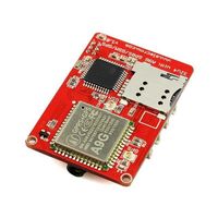
Anti-Theft TV Laptop Mini GPS Tracking Device GT01 Mini GSM GPS Tracker PCBA Board for Bicycle/Motorcycle/Scooter/Vehicle

-
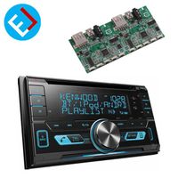
El Car Radio Smt/Dip Car Equipment Multilayer PCB Control Board Prototype Car Radio Pcba Assembly
-
PCB Manufacturer 94v0 Scrap PCBA Manufacturer PCB Board
-
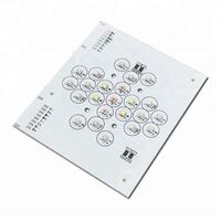
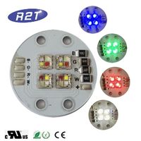
CREE XML Full Color RGBW SMD5050 LED Light PCB Board Assembly
-
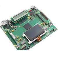
Mega2560 ATMEGA16U2 / Pro Mini MEGA 2560 Mega+WiFi R3 ATmega2560 CH340G Chip For Arduino UNO R3 WeMos ESP8266 Development Board
-
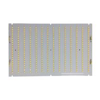
High Efficiency LM281B+ VK Pro LED PCB Board
-
Pulse Induction Metal Detector PI Metal Detector PCBA Assembly
-
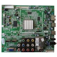
Professional pcb manufacturing for samsung tv spare parts
-
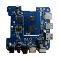
4GB Ram 32GB 64GB Rom 4k Internet Pcba S905X BGA388 AMLOGIC 905X S905 CPU S905 BGA Quad Core 64-bit Chip New Original Sold
-
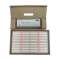
Custom LED board for LED grow light

Other Products
-
$8.00 / piece
-
$4.50 / piece