- Products
- Products
- Companies
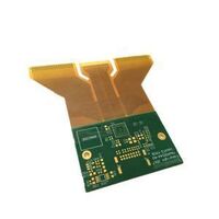
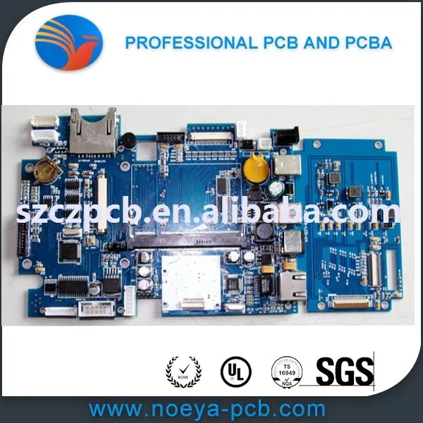
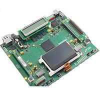
1th s Bitcoin Mine UL 94v0 Pcb Board Manufacturer

-
Supplier: Shenzhen Noeya Technology Co., Ltd. -
Region: Guangdong, China -
Contact: Ms Mary Hu -
Price: $0.50 / >=10 pieces -
Min. Order: 10 pieces
| Tolerance of Etching: | ±1mil(±25um); | Port: | Shenzhen; |
| Board Thickness: | 1.6mm; | Base Material: | FR-4; |
| Packaging Detail: | Vacuum+Dessicant or Sealing package+carton; | Twist&Wrap: | ≤ 0.5%; |
| Silkscreen: | White/BlackYellow/etc.; | Surface finishing: | Protective coating for pcba; |
| Payment Terms: | T/T,Western Union,ESCROW; | Min. Line Width: | 0.1mm; |
| Supply Ability: | 50000 Square Meter/Square Meters per Week pcba; | Certificate: | ROHS,UL,SGS,ISO/TS16949,ISO14001:2004; |
| Solder mask: | Green. Red. Blue. White. Black.Yellow; | Model Number: | NYY-01-PCB-003; |
| Brand Name: | NOEYA; | Files: | Gerber,protel,powerpcb,Autocad,etc.; |
| PCBA Assembly: | OEM/ODM; | Surface Finishing: | HASL/ENIG/Immersion Silver/OSP; |
| Place of Origin: | Guangdong China (Mainland); | Min. Hole Size: | 0.1mm; |
| PTH copper thickness: | 0.4-2mil(10-50um); | Min. Core Thickness: | 0.075mm; |
| Copper Thickness: | 1oz; | Min. Line Spacing: | 0.1mm; |
1th s Bitcoin Mine UL 94v0 Pcb Board Manufacturer
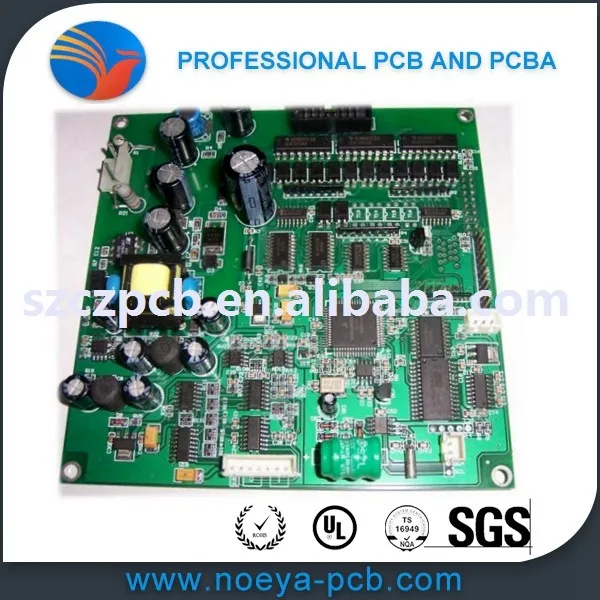
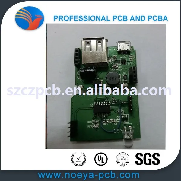
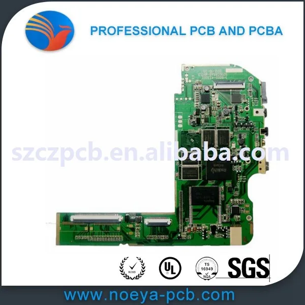
Product Description |
1.NOEYA PCB ASSEMBLY CAPABILITY
Quantity | Prototype&Low Volume PCB Assembly,from 1 Board to 250,is specialty,or up to 1000 |
Type of Assembly | SMT,Thru-hole |
Solder Type | Water Soluble Solder Paste,Leaded and Lead-Free |
Components | Passive Down to 0201 size BGA and VFBGA Leadless Chip Carriers/CSP Double-sided SMT Assembly Fine Pitch to 0.8mils BGA Repair and Reball Part Removal and Replacement |
Bare Board Size | Smallest:0.25*0.25 inches Largest:20*20 inches |
File Formate | Bill of Materials Gerber files Pick-N-Place file |
Types of Service | Turn-key,partial turn-key or consignment |
Component packaging | Cut Tape,Tube,Reels,Loose Parts |
Turn Time | Same day service to 15 days service |
Testing | Flying Probe Test,X-ray Inspection AOI Test |
PCB assembly process | Drilling-----Exposure-----Plating-----Etaching & Stripping-----Punching-----Electrical Testing-----SMT-----Wave Soldering-----Assembling-----ICT-----Function Testing-----Temperature & Humidity Testing |
----Professional Surface-mounting and Through-hole soldering Technology
----Various sizes like 1206,0805,0603 components SMT technology
----ICT(In Circuit Test),FCT(Functional Circuit Test) technology.
----PCB Assembly With UL,CE,FCC,Rohs Approval
----Nitrogen gas reflow soldering technology for SMT.
----High Standard SMT&Solder Assembly Line
----High density interconnected board placement technology capacity.
2.NOEYA PCB CAPABILITY:
Item | Capability | |
1.Base Material | FR-1/FR-4 / High TG FR-4 / Lead free Materials (ROHS Compliant) / Halogen Free material /CEM-3/CEM-1/ /PTFE/ROGERS/ARLON/TACONIC FPC | |
2.Layers | 1-24 | |
3.Finised inner/outer copper thickness | 1-6OZ | |
4.Finished board thickness | 0.2-7.0mm | |
Tolerance | Board thickness≤1.0mm: +/-0.1mm 1 Board thickness>2.0mm: +/-8%
| |
5.Max panel size | ≤2sidesPCB: 600*1500mm Multilayer PCB: 500*1200mm
| |
6.Min conductor line width/spacing | Inner layers: ≥3/3mil Outer layers: ≥3.5/3.5mil
| |
7.Min hole size | Mechanical hole: 0.15mm Laser hole: 0.1mm
| |
Drilling precision: first drilling | First drilling: 1mil Second drilling: 4mil
| |
8.Warpage | Board thickness≤0.79mm: β≤1.0% 0.80≤Board thickness≤2.4mm: β≤0.7% Board thickness≥2.5mm: β≤0.5%
| |
9.Controlled Impedance | +/-5% | |
10. Aspect Ratio | 15:1 | |
11.Min welding ring | 4mil | |
12.Min solder mask bridge | ≥0.08mm | |
13.Plugging vias capability | 0.2-0.8mm | |
14. Hole tolerance | PTH: +/-3mil NPTH: +/-2mil
| |
15.Outline profile | Rout/ V-cut/ Bridge/ Stamp hole | |
16.Surface treatment | OSP: 0.5-0.5um HASL: 2-40um Lead free HASL: 2-40um ENIG: Au 1-10U’’ ENEPIG: PB 2-5U’’/ Au 1-8U’’ Immersion Tin:0.8-1.2um Immersion silver: 0.1-1.2um Peelable blue mask Carbon ink Gold plating: Au 1-150U’’
| |
17. E-testing pass percent | 97% pass for the first time,+/-2%(tolerance) | |
FQC-Physical Lab: Reliability tests | ||
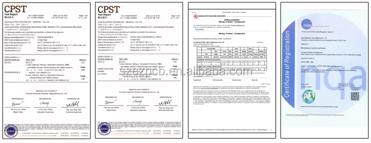
18.Certificate | UL,SGS,ROHS,ISO/TS16949,ISO14001:2004 | |
|
| |
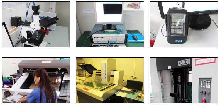
Our equipments | ||
1.Drilling workshop | 4 drilling bits of drilling machine: 4 sets 2 drilling bits of drilling machine: 2 sets
| |
2. photo plotting workshop | Israel “ORBOTECH” Photo Plotters | |
3.AOI | AOI machine | |
4.IPQC | “OXFORD” CMI 700 Copper Thickness Tester | |
5.Impedance test | USA “Tektronix” DSA 8200 Impedance Tester | |
6.Outline workshop | CNC routing machine: 7 sets angle-cutting machine V-cut machine
| |
7.Testing Workshop | Surpass X-600: 2sets WTD FT-2808: 5sets WTD HV300: 1set
| |
8.X-ray | X-ray machine | |
Acceptable file format | ||
GERBER file, PROTEL series, PADS series, POWER PCB series, AutoCAD series. | ||
3.FLOW CHART:

Packaging and Shipping |
Shipping:

Payment:

Company Information |
Company Profile:
Noeya can reliably manufacture up to 8 layer,the material, FR4,FR-1(94V0,94HB)and CEM-1 are all available for us. all pcb with these base material are at competitive prices. We also offer mixed board multilayer panels to ensure your prototyping costs are kept to a minimum. We are able to produce Prototype, and Medium to Large Production Runs with short lead times - 5 Days is considered normal for the majority of these jobs, and can build PCB boards for you using non-leaded surface finishes that are RoHS compliant.
Our manufacturing capacity of the company was expanded rapidly. Double-side and multi-layer PCB (1L-8L)with high and accurate yearly output is over 800, 000 square meters, and most of our products have been sold to the market of Europe, North America, South America and Australia.We have enjoyed good reputation among the same occupations both at home and abroad for our professional manufacturing technology, stable product quality and exquisite craftsmanship measure.
Our products main application area is: Medical Instrumentation, Telecommunication apparatus, industry power, Automotive, Liquid crystal module, Peripherals, Computing & storage, Consumer, Networking, satellite receiver (DVB), worker person who accuse of Hi-Tech trade is it produce and design the technological service to offer.
Until now, we won ISO9001-2000 Quality Management System authentication and all the products were passed UL certificate. Since built our office in Shenzhen, we have been expanding our overseas markets, especially tending to the Emerging markets: like South America (Brazil), and mid-east, all because of our price advantage.
Foundation of our company, we have concentrated on the craftsmanship development and made efforts to upgrade the technology level and manufacturing capacity in the professional field of PCB, OEM and finally we achieved good results. We consider every client as our gods, we can meet all our clients requirements whether the order is sizable or small or prototype.
Access To The Website >>>>
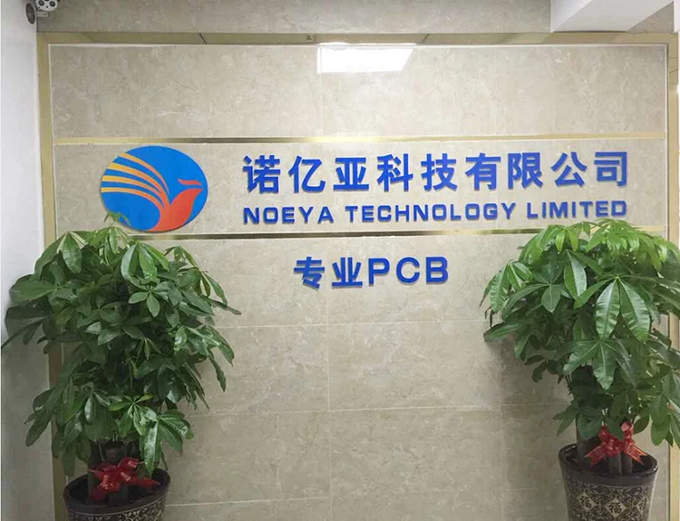
Our Factory:

Testing Equipment:
Our Certification:
FAQ |
1.Which type of PCBs do you expert in?
We are specialized in producing HDI multilayer blind, BGA, impedance, half-hole, double-sided, single-sided, etc.
2.Experience?
We are OEM on PCB boards with experience over 9 years.
3.What is your Lead time?
Lead time is usually punctual here, for some special situation, we can also advise customer in advance to avoid any inexpectation or loss at customer side.
4.What is your testing policy and how you controle the quality?
For sample, usually tested by flying probe; for PCB Volume over 3 square meters, usually tested by fixture, this will be more faster. Due to there’s many steps to PCB production, we usually do inspection after every step.
5.What is your certificate?
ISO/TS16949: 2000, ISO14001: 2004, UL, SGS, CE&RoHS report. We can provide the report of raw material based on customer’s requirement.
6.What is your package?
With Inner vacuum package and out carton.
7.PCB shipment?
This is depend on customer, sometimes we ship through our forwarder, who is also the agency of DHL, TNT, UPS, Fedex, and so on. Our forwarder can provide too much better freight cost than we get directly from those express enterprise.
8.What is your produce ability?
Our ability is average 40,000 square meters per month.
9.I only have the pcb sample, not pcb file, can you produce it for me?
Yes, we can copy file based on your sample, this file names gerber, and production then is accorded to gerber file.
10.Can you design gerber file?
We can design gerber file if customer can provide us schematic, schematic sample can also be provided if customer want.
11.What kind of PCB file format can you accept for production? What CAM software do you use?
We accept Gerber file for production. CAM350, GENESIS, UCAM, GC-CAM, V-2000.
12.Will you allow me to put several part number together into one panel?
Yes, this is usually happen in we factory, this way can help customers reduce some cost and to a certain degree, it can help reduce some assembly cost.
13.What material brand you use for your PCB?
KB, SL, NANYA, TACONIC, ROGERS and so on.
14.What is your minimum order quantity?
We have no limitation on MOQ, prototype, medium volume and large volume are all acceptable.
15.Will RoHS Lead-Free Custom Spec. Boards be marked with lead-free symbol?
Yes, can, but need customer to specify this requirement in file.
16.Are my design files safe when I submit them to you for manufacturing?
Any customer’s file will be protected very well here in our factory and we will not let any third party know. We can sign NDA with you.
17.Quotation requirement for PCB Assembly ?
Experienced pcb
circt board
assembly manufacturer

Experienced pcb
circuit board
assembly manufacturer
-
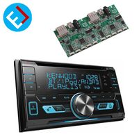
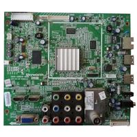
Anti-Theft TV Laptop Mini GPS Tracking Device GT01 Mini GSM GPS Tracker PCBA Board for Bicycle/Motorcycle/Scooter/Vehicle

-
El Car Radio Smt/Dip Car Equipment Multilayer PCB Control Board Prototype Car Radio Pcba Assembly
-
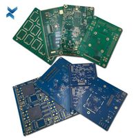
PCB Manufacturer 94v0 Scrap PCBA Manufacturer PCB Board
-
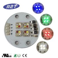
CREE XML Full Color RGBW SMD5050 LED Light PCB Board Assembly
-
Mega2560 ATMEGA16U2 / Pro Mini MEGA 2560 Mega+WiFi R3 ATmega2560 CH340G Chip For Arduino UNO R3 WeMos ESP8266 Development Board
-
High Efficiency LM281B+ VK Pro LED PCB Board
-
Pulse Induction Metal Detector PI Metal Detector PCBA Assembly
-
Professional pcb manufacturing for samsung tv spare parts
-
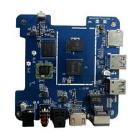
4GB Ram 32GB 64GB Rom 4k Internet Pcba S905X BGA388 AMLOGIC 905X S905 CPU S905 BGA Quad Core 64-bit Chip New Original Sold
-
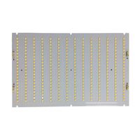
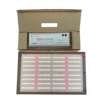
Custom LED board for LED grow light

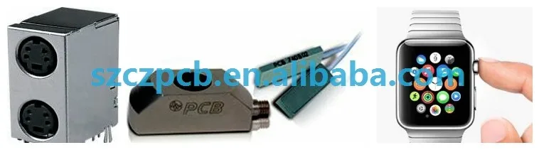
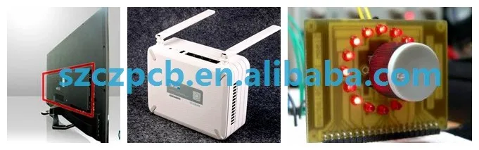
Other Products
-
$0.10 / piece