- Products
- Products
- Companies
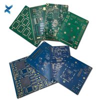
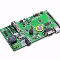
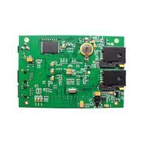
Shenzhen PCB PCBA Custom Service High Quality Led Panel Led Panel Light

-
Supplier: Shenzhen Xinjiaye Electronics Technology Co., Ltd. -
Region: Guangdong, China -
Contact: Mr Gail Peng -
Price: $1.00 /piece -
Min. Order: 1 piece
Product details
| Certificates: | UL ROHS ISO9001 ISO14001; | Maximun size: | 500mm*800mm; |
| Base Material: | FR4; | Type: | Panel manufacture; |
| Insulation Layer Thickness: | 0.075mm-5.0mm; | Brand Name: | XJY; |
| Port: | Shenzhen; | Copper Thickness: | 1oz; |
| Aspect Ratio: | 13:1; | Solder Mask: | Green, blue, red, white, black, etc; |
| Surface Finishing: | LF-HASL; | Board Thickness: | 1.6mm; |
| Layer counts: | 2-16; | Payment Terms: | L/C,D/A,D/P,T/T,Western Union,MoneyGram,paypal; |
| Place of Origin: | Guangdong China; | Min. Line Spacing: | 5 Mil; |
| Min. Hole Size: | 0.15mm; | Supply Ability: | 10000 Piece/Pieces per Month; |
| Packing: | Vacuum or carton; | Test: | AOI; |
| Packaging Detail: | Packaging Detail:Pcb inner packing:vacuum plastic packing Pcb outer packing :standard caron packing; | Model Number: | JY PCB; |
| Plus Via Diameter: | 0.25mm-0.60mm; | Min. Line Width: | 0.075(3mil); |
power supply ul 94vo pcb dc ac inverter pcb bare pcb atmega8 48 88 168 minimum system board
Skype:+8615107111605
Company Information
Shenzhen XinJiaYe Electronics Technology Co,.Itd.
- XJYPCB Manufacturer is a professional pcb manufacturer has over 10 years experience;
- we are able to offer customized pcb ranging from pcb board, aluminium pcb, flexible pcb, high frequency pcb, components purchase, pcb asse mbly, pcb copy service;
- Our products are widely used in communication apparatus, automobile electronics, auto parts, computers, medical devices, light systems, outdoor systems, network devices and consumer electronics class fields, ect.
| Item | Capability | Item | Capability |
| Layers | 1-28 | Thicker Copper | 1-6oz |
| Products Type | HF(High-Frequency)&(Radio Frequency) board, Imedance controlled board,HDI board, BGA& Fine pitch board | solder mask | Nanya&Taiyo, LPI&Matt red, green,yellow,white,blue,black. |
| Base Material | FR4(Shengyi China, ITEQ, KB A+,HZ),HI-TG,Fr06,Rogers,Taconic,Argon,Naclo,Isola and so on | Finished Surface | Conventional HASL, Lead-Free HASL,Flash Gold,ENIG(Immersion Gold),OSP(Entek),Immersion Tin, Immersion Sliver, Hard Gold |
| Selective Surface Treatment | EING(Immersion Gold)+OSP, ENIG(Immersion Gold)+Gold Finger, Flash Gold Finger, Immersion Sliver+Gold Finger, Immersion Tin+Gold Finger | ||
| Technical Specification | Minimum line width/gap | 3.5/4mil(laser dirll) | |
| Minimum hole size | 0.15mm(mechanical dirll) 4mil(laser dirll) | ||
| Minimum Annular Ring | 4mil | ||
| Max Copper Thickness | 6oz | ||
| Max Production Size | 600mm*800mm | ||
| Board Thickness | D/S:0.2-7.0mm, Multilayer:0.4-7.0mm | ||
| Min Solder Mask Bridge | ≥0.08mm | ||
| Aspect Ratio | 15:1 | ||
| Plugging Vias Capability | 0.2-0.8mm | ||
| Tolerance | Plated holes Tolerance | ±0.08mm(min±0.05) | |
| Non-Plated Hole Tolerance | ±0.05mm(min+0/-0.05mm or +0.05/-0mm) | ||
| Outline Tolerance | ±0.15mil(min±0.10mm) | ||
| Functional Test | |||
| Insulating Resistance | 50ohms(normality) | ||
| Peel Off Strength | 1.4N/mm | ||
| Thermal Stress Test | 265℃,20seconds | ||
| Solder Mask Hardness | 6H | ||
| E-test Voltage | 500V+15/-0V 30s | ||
| Warp and Twist | |||
Our service
PCB Features
- Low water absorption rate
- Hard to be deformed
- High mechanical strength
- Good electric performance wether under the moist or dry environment, Flame retardant grade could reach 94-V0
- High temperature resistant,high dielectric performance and mechanical processing performance.
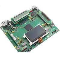
PCB manufacture and PCB assembly
- PCB board file with parts list provided by customer
- PCB board made, circuit board parts purchased by us
- PCB board with parts assembled
- Electronic testing circuit board or PCB
- Fast delivery, anti-static package
- RoHS Directive-compliant, lead-free
- One stop service for PCB design, PCB layout, PCB manufacture, components purchasing, PCB assembly, test, packing and PCBdelivery
PCB manufacture Technical Requirement
- Professional Surface-mounting and Through-hole soldering Technology
- Various sizes components SMT technology
- FCT(Functional Circuit Test) technology Electronic Products High Quality pcb connector iphone Made In China
- PCB Assembly With UL,Rohs Approval
- Nitrogen gas reflow soldering technology for SMT
- High Standard SMT&Solder Assembly Line
- High density interconnected board placement technology capacity
Testing Procedures For PCB Board
- Visual Inspection
- Flying probe
- Impedance control
- Solder-ability detection
- Digital metallograghic microscope
- AOI (Automated Optical Inspection)
Shipping Note
- Sample spares for quality testing, micro-section test is avaible,
- Email notification with tracking number once shipment was arranged
- For any issues during the shipment to customers' end advising and follow-up
FAQ
How to get a quote?
- --- Pls send BOM and gerber file with these format: .PCB / .P-CAD / .DXP / .CAD / .Gerber
- Base material: FR4/ AL/ FPC/ CEM-1/ CEM-3/ 94v0/ Rogers
- Board thickness: 1.6mm-3.2mm/ 0.3mm-1.2mm
- Copper thickness: Hoz/ 1oz/ 2oz/ 3oz/ 4oz, ect
- Surface treatment: HASL/ ENIG/ LF-HAL/ Immersion Tin/ Immersion Sin/ OSP
- color of solder mask and silkscreen: Green/White/Black/Red/Blue/Yellow
- Quantity and board size
What we need
- For PCB enquiry, gerber file or any other pcb production file is needed. Any details are also welcomed if no Gerber file
- such as schematic or a sample.
- For PCBA enquiry,BOM(Bill of Materials) is needed besides.
- Reverse engineering and PCB clone services are available if given a sample
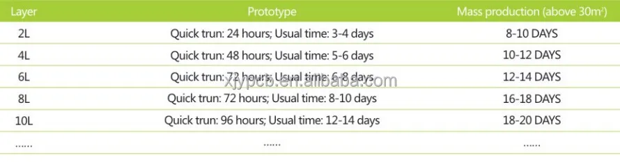
Lead Time
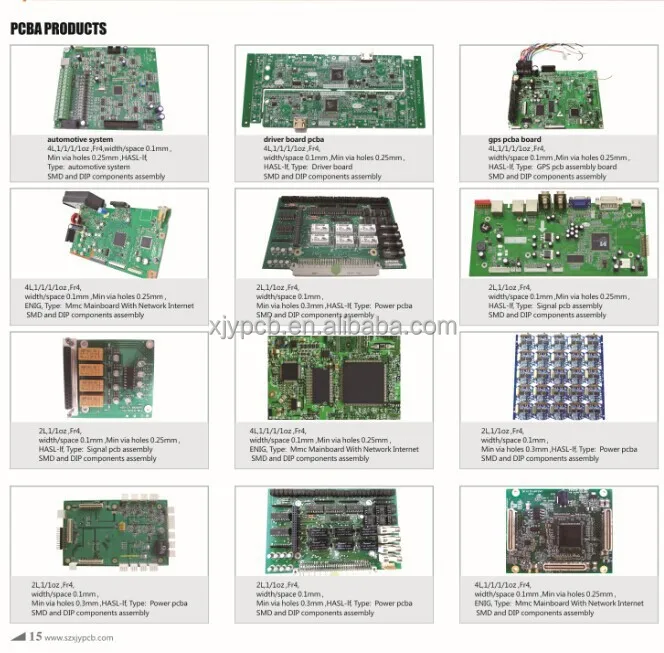
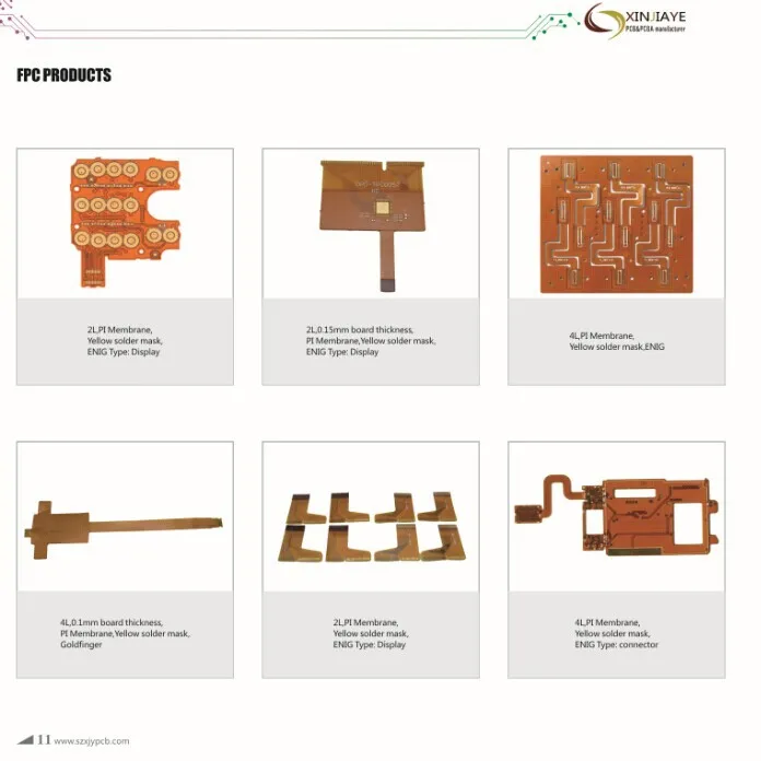
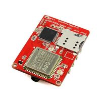
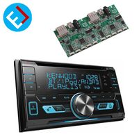
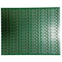
Products Show


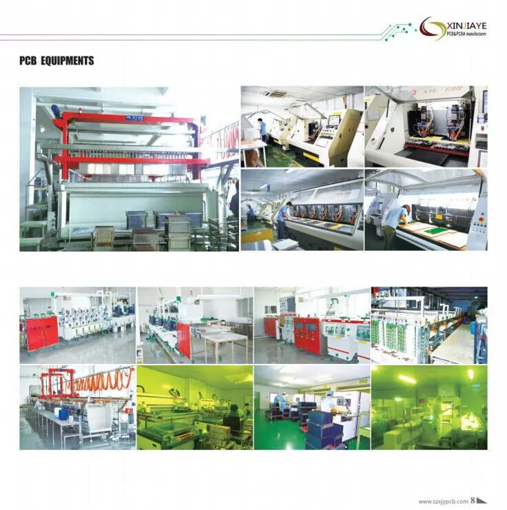
Equipments
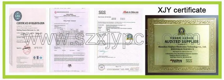
Certifications
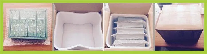
Packaging & Shipping
VIEW MORE
You may like
-
Anti-Theft TV Laptop Mini GPS Tracking Device GT01 Mini GSM GPS Tracker PCBA Board for Bicycle/Motorcycle/Scooter/Vehicle

-
El Car Radio Smt/Dip Car Equipment Multilayer PCB Control Board Prototype Car Radio Pcba Assembly
-
PCB Manufacturer 94v0 Scrap PCBA Manufacturer PCB Board
-
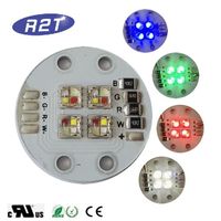
CREE XML Full Color RGBW SMD5050 LED Light PCB Board Assembly
-
Mega2560 ATMEGA16U2 / Pro Mini MEGA 2560 Mega+WiFi R3 ATmega2560 CH340G Chip For Arduino UNO R3 WeMos ESP8266 Development Board
-
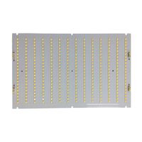
High Efficiency LM281B+ VK Pro LED PCB Board
-
Pulse Induction Metal Detector PI Metal Detector PCBA Assembly
-
Professional pcb manufacturing for samsung tv spare parts
-
4GB Ram 32GB 64GB Rom 4k Internet Pcba S905X BGA388 AMLOGIC 905X S905 CPU S905 BGA Quad Core 64-bit Chip New Original Sold
-
Custom LED board for LED grow light

Other Products
-
$1.00 / piece
-
$0.01 / piece
-
$0.01 / piece
-
$0.10 / piece
-
$0.01 / piece
Related Search
high quality led alu pcb
high quality led daytime turn running light
high quality led screen board for advertising
high power led navig light suppliers
high power led fog lights
outdoor high power led street light
aluminum 5w high power led down light
high quality universal pcb leds
high quality car led lighting
high quality a60 led bulb 12w