- Products
- Products
- Companies
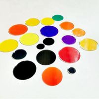
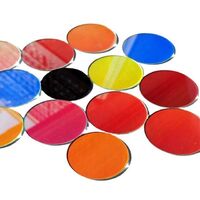
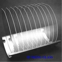
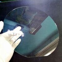
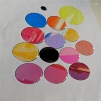
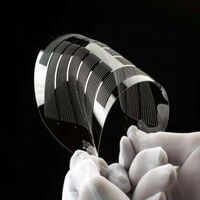
8'' glass wafer borosilicate 3.3 for semiconductor

-
Supplier: Xinyu Tking Glass Co., Ltd. -
Region: Jiangxi, China -
Contact: Ms Spring Lin -
Price: $10.00 / >=50 pieces -
Min. Order: 50 pieces
| Supply Ability: | 5000 Piece/Pieces per Month; | Thickness2: | 1.0mm 2.0mm 3mm 4mm 5mm 6mm 7mm 8mm; |
| Thcikness: | 0.1mm 0.2mm 0.3mm 0.5mm 0.7mm 1.1mm; | Glass material: | Borofloat33,Corning Eagle Xg , Quartz glass ,Corning Willow glass; |
| Glass material2: | Soda lime glass, Borosilicate glass; | Packaging Detail: | Porfessional export packing; |
| Payment Terms: | L/C,D/P,T/T,Western Union,MoneyGram; | Size: | 2'' 3'' 4'' 6'' 8'' 12''; |
| Light transmission: | 92%; | Place of Origin: | Jiangxi China; |
| Port: | Guangzhou; | Model Number: | Tk01; |
| Temperature resistant: | 550degree C; | Brand Name: | Tking; |
| Polishing: | Both sides or one side polishing; |
| Attribute |
Measurements |
|
Diameter |
Φ2",Φ3",Φ4",Φ5",Φ6",Φ8",Φ12" |
|
Thickness |
0.2mm,0.3mm,0.4mm,0.5mm,0.7mm,1.0mm,1.5mm tolerance±0.02mm) |
|
Dimensional Tolerance |
+/- 0.02 |
|
Thickness Tolerance |
+/- 5μm |
|
Thickness Variation (TTV) |
< 0.01mm |
|
Flatness |
1/10 Wave/Inch |
|
Surface Roughness (RMS) |
<1.5nm |
|
Scratch and Dig |
5/2 |
|
Particle Size |
<5μm |
|
Bow/Warp |
<10μm |
The following describes the versatility within several of our key processes. For full details on the process, please contact us freely get more information.
WAFER FABRICATION PROCESS
Shape Cut
Thin sheets are scribed, thick sheets are water jetted and blocks are wire sawn to begin the process with a wafer “blank”.
CNC Edge
Each wafer is individually edged on a Precision CNC Edge Grinding Station.
Lapping
As required, wafers are lapped to precise thickness or flatness.
Polishing
Double-side Commercial Polish removes subsurface damage and Super Polish creates a pristine finish.
Cleaning
We combine ultrasonics and megasonics on multiple cleaning lines which feed directly into a Class 100 Clean Room.
Inspection
In our Class 100 Optical Clean Room, we inspect to various quality levels under the appropriate lighting conditions.
Packaging
All wafers are packed in pre-cleaned containers, double bagged and vacuum sealed within the Class 100 Clean Room.


WAFER SPECIFICATIONS
Tking produces wafers to all SEMI Standards including dimensional, flat and notch specifications. In addition, we offer custom specifications designed to your unique needs including, alignment marks, holes, pockets, edge profile, thickness, flatness, surface quality, cleanliness or any other details critical to your application. We also offer these wafers in a broad array of materials including Borosilicate, Aluminosilicate, Fused Silica (instead of quartz), Quartz and Soda Lime.
-
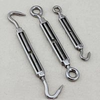
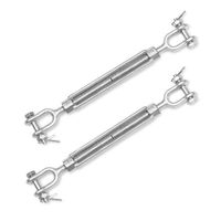
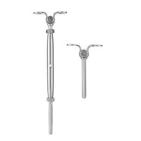
JIS type turnbuckle eye & eye highly polished stainless steel AISI316, for assembly with wire rope

-
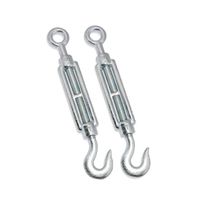
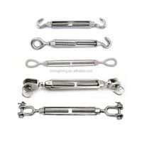
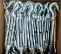
Factory Low Price ASTM F1145-92 Forged Turnbuckle Screws China Galvanized Eye Claw Eye Hook Turnbuckle Screws
-
DIN1480 hook and eye turnbuckle hot selling Q235 hook eye type forged steel galvanized DIN1480 turnbuckle
-
Turnbuckle hot selling Q235 hook eye type forged steel galvanized DIN1480 turnbuckle
-
Custom Wire Rope Tensioning Stainless Steel Frame Eye Hook Turnbuckle Screws
-
Hot-dip galvanized forging cable turnbuckle American turnbuckle screw claw turnbuckle screw
-
Stainless Steel 316 Deck Toggle and Swaged Stud Turnbuckle Terminal Enclosed Body Turnbuckle Rigging American Style
-
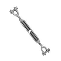
AISI304/AISI316 stainless steel open body turnbuckles, customized standard or non-standard wire rope turnbuckles
-
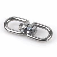
Double ring swivel with stainless steel fittings
-
Linyi Rigging Galvanized Malleable Iron Din1480 bend

Other Products
-
$2.00 / piece
-
$1.50 / piece
-
$8.00 / piece
-
$7500.00 / set
-
$10.00 / piece
-
$1.50 / piece
-
$8.00 / piece
-
$1.00 / piece